Femtosecond-laser and two-photon polymerization micro-nano machining system and method

A two-photon polymerization, femtosecond laser technology, applied in microlithography exposure equipment, optics, optomechanical equipment, etc., can solve the problem of limited improvement in processing efficiency of three-dimensional micro-nano devices, high difficulty in mass production of three-dimensional micro-nano devices, displacement In order to improve the processing efficiency and process flow, reduce the positioning accuracy requirements, and simplify the processing technology

Active Publication Date: 2014-11-19
SOUTH UNIVERSITY OF SCIENCE AND TECHNOLOGY OF CHINA
View PDF1 Cites 14 Cited by
  • Summary
  • Abstract
  • Description
  • Claims
  • Application Information

AI Technical Summary

Problems solved by technology

[0006] However, the above-mentioned multi-focus parallel processing method is more suitable for mass production of micro-nano devices with periodic structures, but it is still very difficult to mass-produce arbitrarily complex three-dimensional micro-nano devices
During the processing, the focus of each beam of light still needs to move point by point according to the pre-designed trajectory. Usually, the relative displacement between the focus of the femtosecond laser and the photosensitive material is realized by controlling the movement of the translation stage, and the inertia of the translation stage is large, and the response It takes a long time. Therefore, the existing multi-focus parallel processing method has limited improvement in the processing efficiency of making any complex three-dimensional micro-nano devices, and requires high-precision mechanical positioning capabilities in three-dimensional directions, which increases the processing difficulty.

Method used


Image

  • Femtosecond-laser and two-photon polymerization micro-nano machining system and method
  • Femtosecond-laser and two-photon polymerization micro-nano machining system and method
  • Femtosecond-laser and two-photon polymerization micro-nano machining system and method

Examples


Embodiment 1

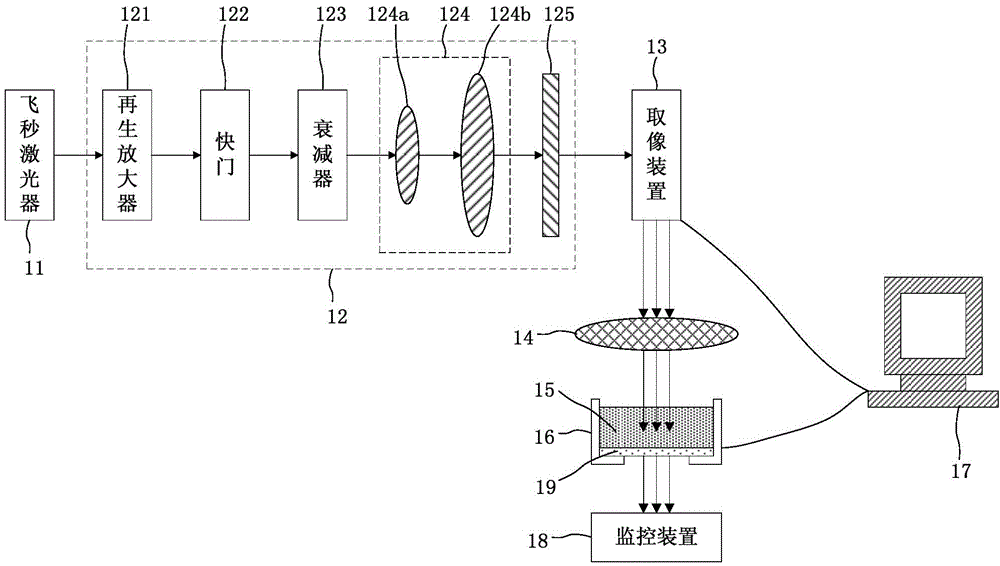
[0042] Embodiment 1 of the present invention provides a femtosecond laser two-photon polymerization micro-nano processing system. figure 1 It is a schematic structural diagram of a femtosecond laser two-photon polymerization micro-nano processing system provided in Embodiment 1 of the present invention. Such as figure 1As shown, the femtosecond laser two-photon polymerization micro-nano processing system includes: femtosecond laser 11, used to generate femtosecond laser; external optical path modulation unit 12, used to modulate the femtosecond laser; image taking device 13 , for taking images of the cross-sectional patterns of the three-dimensional micro-nano device layer by layer, so that the modulated femtosecond laser forms parallel beams arranged according to the cross-sectional patterns of each layer; the focusing lens 14 is used for The parallel light beams arranged in the cross-sectional pattern are respectively focused in the photosensitive material 15 to form a plan...

Embodiment 2

[0050] Embodiment 2 of the present invention also provides a femtosecond laser two-photon polymerization micro-nano processing system. On the basis of the first embodiment, the imaging device of this embodiment adopts a dynamic imaging device.

[0051] In this embodiment, the computer 17 is used to control the imaging device, including: the computer is used to model the structure of the three-dimensional micro-nano device, and convert the model obtained by modeling into The digital voltage signal is loaded on the dynamic imaging device to form cross-sectional patterns of each layer of the three-dimensional micro-nano device on the dynamic imaging device. Specifically, the computer 17 can carry out computer-aided design through the software control unit in it, establish a three-dimensional model for the three-dimensional micro-nano device to be processed, divide the built three-dimensional model into multi-layer cross-sectional graphics, and then divide each layer of cross-sect...

Embodiment 3

[0068] Embodiment 3 of the present invention also provides a femtosecond laser two-photon polymerization micro-nano processing system. Different from the second embodiment, the imaging device of this embodiment adopts a static imaging device.

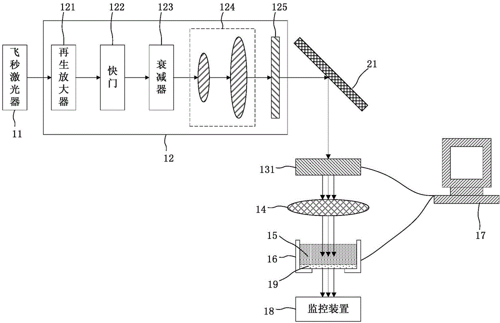
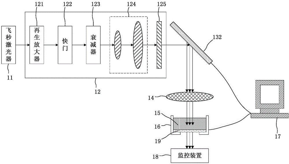
[0069] Further, the static imaging device may use a mask. Figure 4 It is a schematic structural diagram of a femtosecond laser two-photon polymerization micro-nano processing system provided in Embodiment 3 of the present invention. Such as Figure 4 As shown, the static imaging device adopts a mask plate 133, and in order to make the structure of the whole micro-nano processing system more compact, it is set on the advancing path of the femtosecond laser and between the aperture stop 125 and the mask plate 133 imaging device 13 A total reflection mirror 21 is provided.

[0070] In this embodiment, preferably, the mask plate 133 includes a plurality of micro-regions, and each micro-region includes a layer of cross-sectional pattern ...


PUM


Abstract

The invention discloses a femtosecond-laser and two-photon polymerization micro-nano machining system and a femtosecond-laser and two-photon polymerization micro-nano machining method. The micro-nano machining system comprises a femtosecond laser device, a reflector path modulation unit, an image taking device, a focusing lens, a displacement table, a computer and a monitoring device, wherein the image taking device is used for carrying out layer-by-layer image taking on a section graph of a three-dimensional micro-nano device to shape the modulated femtosecond laser into parallel beams arrayed according to the section graph of each layer. According to the femtosecond-laser and two-photon polymerization micro-nano machining system and the femtosecond-laser and two-photon polymerization micro-nano machining method, not only can multiple three-dimensional micro-nano devices be simultaneously machined, but also the arbitrary and complex three-dimensional micro-nano devices can be machined layer-by-layer, so that the machining efficiency and the process flow are improved; besides, in a layer-by-layer micro-nano machining process, the displacement table only needs to move along the thickness direction of the section of the micro-nano device, so that not only can the machining efficiency and the process flow be improved, but also positioning accuracy requirements of the displacement table in two-dimensional directions are reduced, then a machining process is simplified, and the difficulty is reduced.

Description

technical field [0001] The invention relates to the technical field of micro-nano processing, in particular to a femtosecond laser two-photon polymerization micro-nano processing system and method. Background technique [0002] With the development of semiconductor microelectronics technology, various micro-nano processing technologies have become an important research content of modern science and technology. Wide range of applications. [0003] In recent years, with the development of laser technology, two-photon absorption technology using femtosecond laser as light source has been introduced into the field of micro-nano processing. This technology uses a femtosecond laser with a longer wavelength as the light source, and focuses the laser beam on the photosensitive material to be processed through the focusing objective lens. The laser intensity is low, and two-photon absorption does not occur. At the same time, due to the low energy of the laser, the corresponding sin...

Claims


Application Information

Patent Timeline
Patent Type & Authority Applications(China)
IPC IPC(8): G03F7/20
CPCG03F7/0037G03F7/2053G03F7/70041G03F7/70416G03F7/7055G03F7/70641
Inventor 程鑫崔德虎李自平明静
Owner SOUTH UNIVERSITY OF SCIENCE AND TECHNOLOGY OF CHINA
Why Eureka
Try Eureka