

Stable PEDOT/PSS conducting layer electrode and preparing method thereof
A conductive layer, a stable technology, applied in the field of organic optoelectronic technology materials, can solve the problems such as difficult to meet the conductive performance, achieve the effect of simple manufacturing process, reduce equipment and manufacturing costs, and high conductivity
- Summary
- Abstract
- Description
- Claims
- Application Information
AI Technical Summary
Problems solved by technology
Method used
Image

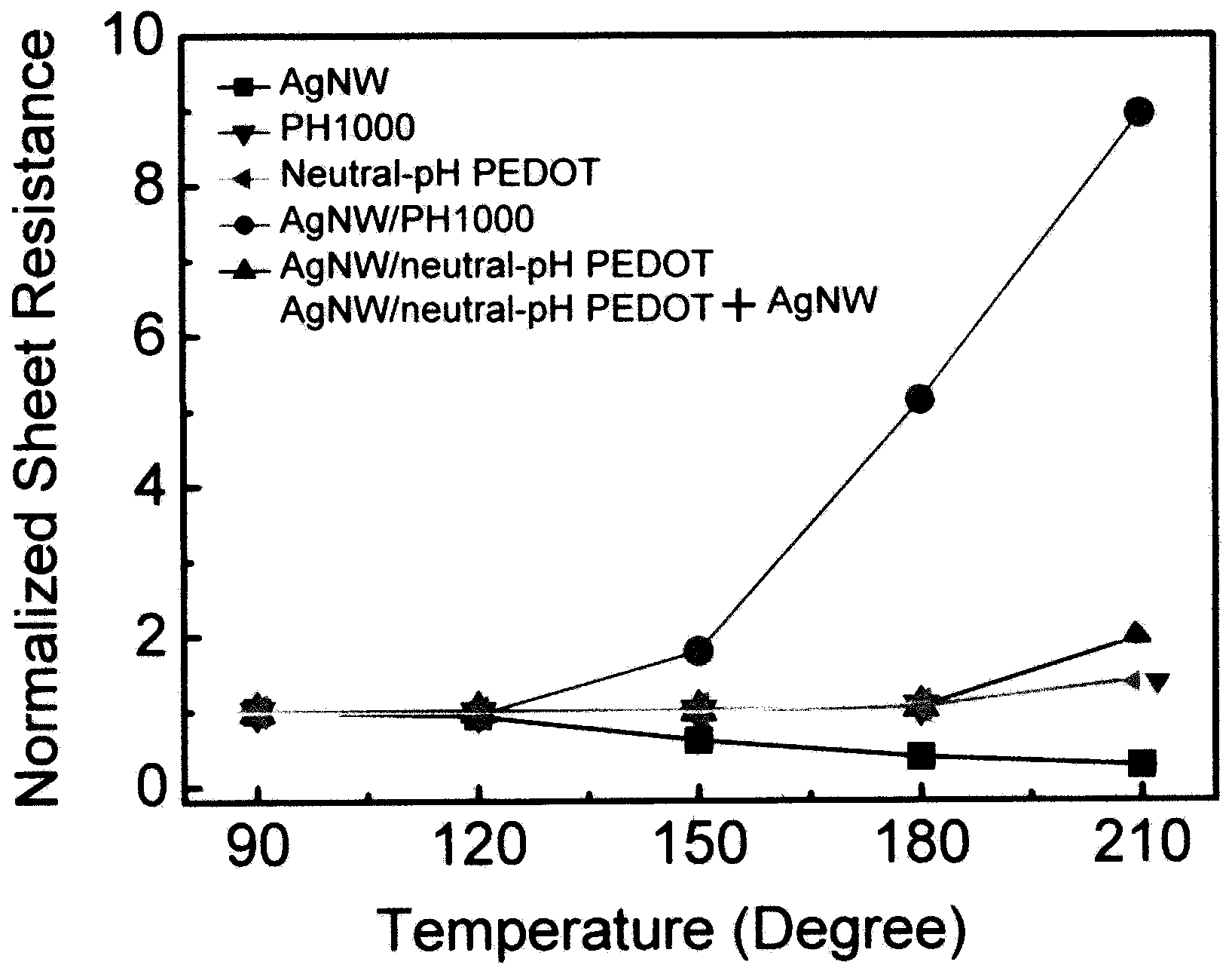
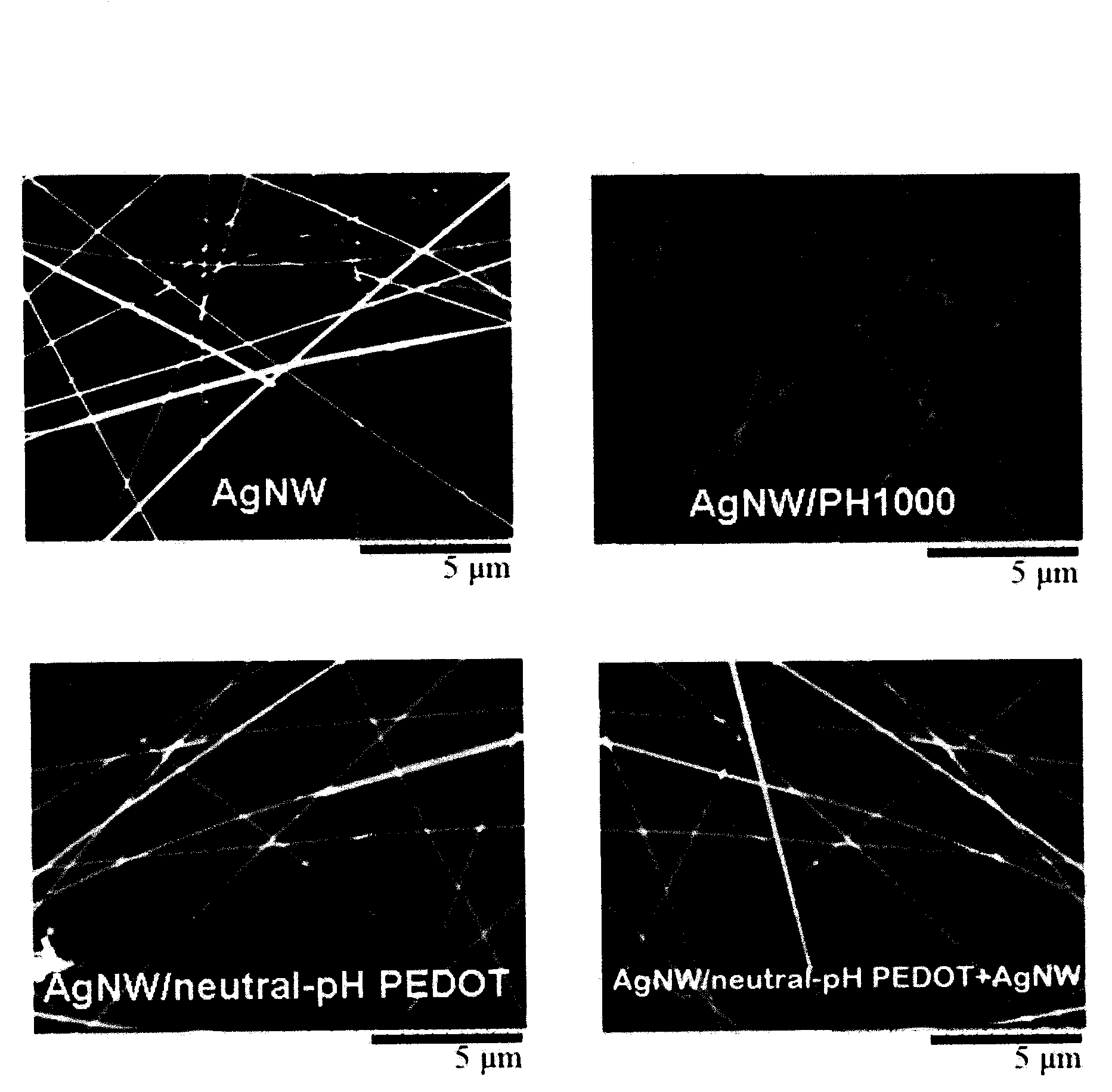
Examples
Embodiment 1
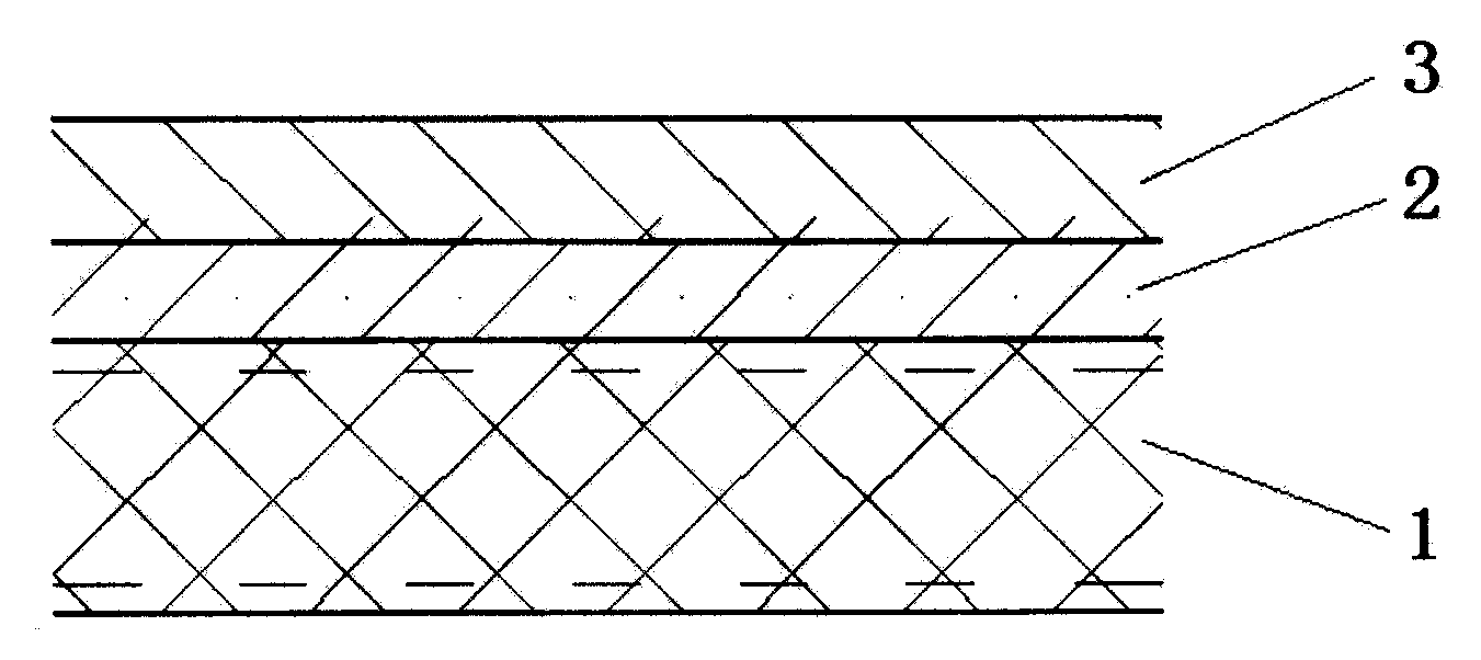
[0054] (1) Carrying out surface pretreatment on the base material, as a transparent base material layer 1 .
[0055] Optical PET film is selected as the base material, and the surface is cleaned before use, followed by cleaning liquid, deionized water, isopropanol and deionized water in an ultrasonic cleaning tank for 10 minutes, and then blowing dry in a nitrogen stream , as the transparent substrate layer 1 .
[0056] (2) Coating and preparing conductive layer 2 of silver nanowires on transparent substrate layer 1 .
[0057] In this example, nano-silver wire conductive ink was selected as the material, and the nano-silver wire conductive ink (XFNANO Agnws-60nm / 20μm isopropanol solvent, containing 5% solids, Nanjing Xianfeng Nano Material Technology Co., Ltd.) was coated on the surface of the transparent substrate layer 1 with a wet film thickness of 12 μm. After coating, the coating was dried at 150° C. for 5 minutes to prepare the silver nanowire conductive layer 2 .
[...
Embodiment 2
[0065] Carry out surface pretreatment to substrate material as transparent substrate layer 1 and on transparent substrate layer 1, the process of preparing nano-silver wire conductive layer 2 is identical with embodiment 1;
[0066] A blend of neutral PEDOT / PSS conductive ink and silver nanowire conductive ink is coated on the nano silver wire conductive layer 2 to form a polymer conductive layer 3 . Wherein, the preparation technology of neutral PEDOT / PSS conductive ink preparation is also identical with embodiment 1;
[0067] The blend of neutral PEDOT / PSS conductive ink used in the present embodiment and nano-silver wire conductive ink, wherein the nano-silver wire conductive ink accounts for 2% by weight of neutral PEDOT / PSS conductive ink;
[0068] Then coat the blend of neutral PEDOT / PSS conductive ink and nano silver wire conductive ink to form polymer conductive layer 3;
[0069]The blend of neutral PEDOT / PSS conductive ink and nano-silver wire conductive ink is print...
PUM
| Property | Measurement | Unit |
|---|---|---|
| Thickness | aaaaa | aaaaa |
| Viscosity | aaaaa | aaaaa |
| Length | aaaaa | aaaaa |
Abstract
Description
Claims
Application Information