
System for improving TSV etching process and etching endpoint monitoring method

An endpoint monitoring and process technology, applied in semiconductor/solid-state device testing/measurement, electrical components, semiconductor/solid-state device manufacturing, etc., can solve problems such as short overlap time, misjudgment of plasma emission intensity, and inability to accurately detect endpoints, etc. Achieve effective monitoring, improve efficiency, extend weight and work time

Active Publication Date: 2014-12-03
ADVANCED MICRO FAB EQUIP INC CHINA
View PDF4 Cites 6 Cited by
  • Summary
  • Abstract
  • Description
  • Claims
  • Application Information

AI Technical Summary

Problems solved by technology

Since the Bosch process uses alternating and repeated isotropic etching and polymer deposition processes, and the plasma conditions (such as process gas type, pressure, RF power, etc.) used in the etching and deposition steps are different, it is necessary to Switch the RF power while switching the process gas; because it takes a certain amount of time for the process gas to be injected into the reaction chamber and reach the required pressure, the overlapping time between the process gas that meets the requirements and the matching RF power is short, and it is difficult to provide stable Etching and deposition protection of the substrate under plasma conditions
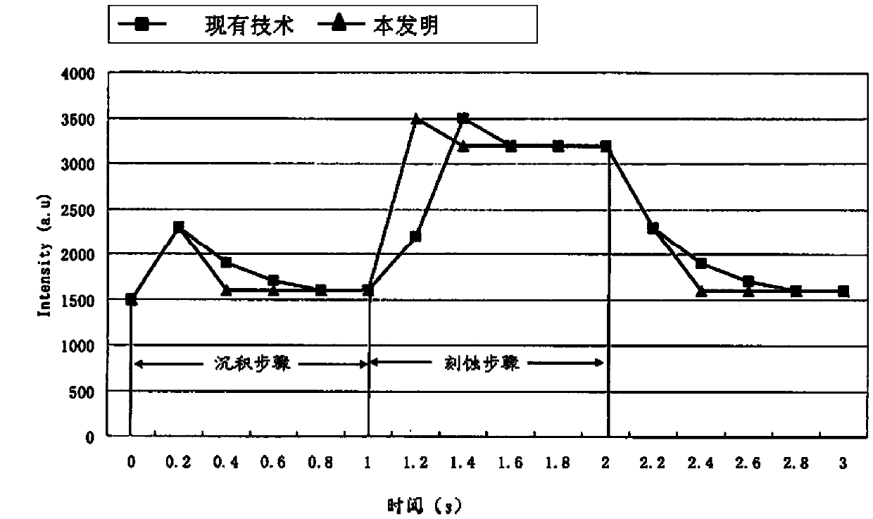
At the same time, applying conventional OES technology to the Bosch process with fast and periodic plasma disturbance characteristics will lead to periodic endpoint trajectories, which are prone to misjudgment of changes in plasma emission intensity, so it cannot accurately detect the endpoint

Method used


Image

  • System for improving TSV etching process and etching endpoint monitoring method
  • System for improving TSV etching process and etching endpoint monitoring method
  • System for improving TSV etching process and etching endpoint monitoring method

Examples


Embodiment Construction

[0025] In order to make the content of the present invention clearer and easier to understand, the content of the present invention will be further described below in conjunction with the accompanying drawings of the specification. Of course, the present invention is not limited to this specific embodiment, and general replacements well known to those skilled in the art are also covered by the protection scope of the present invention.

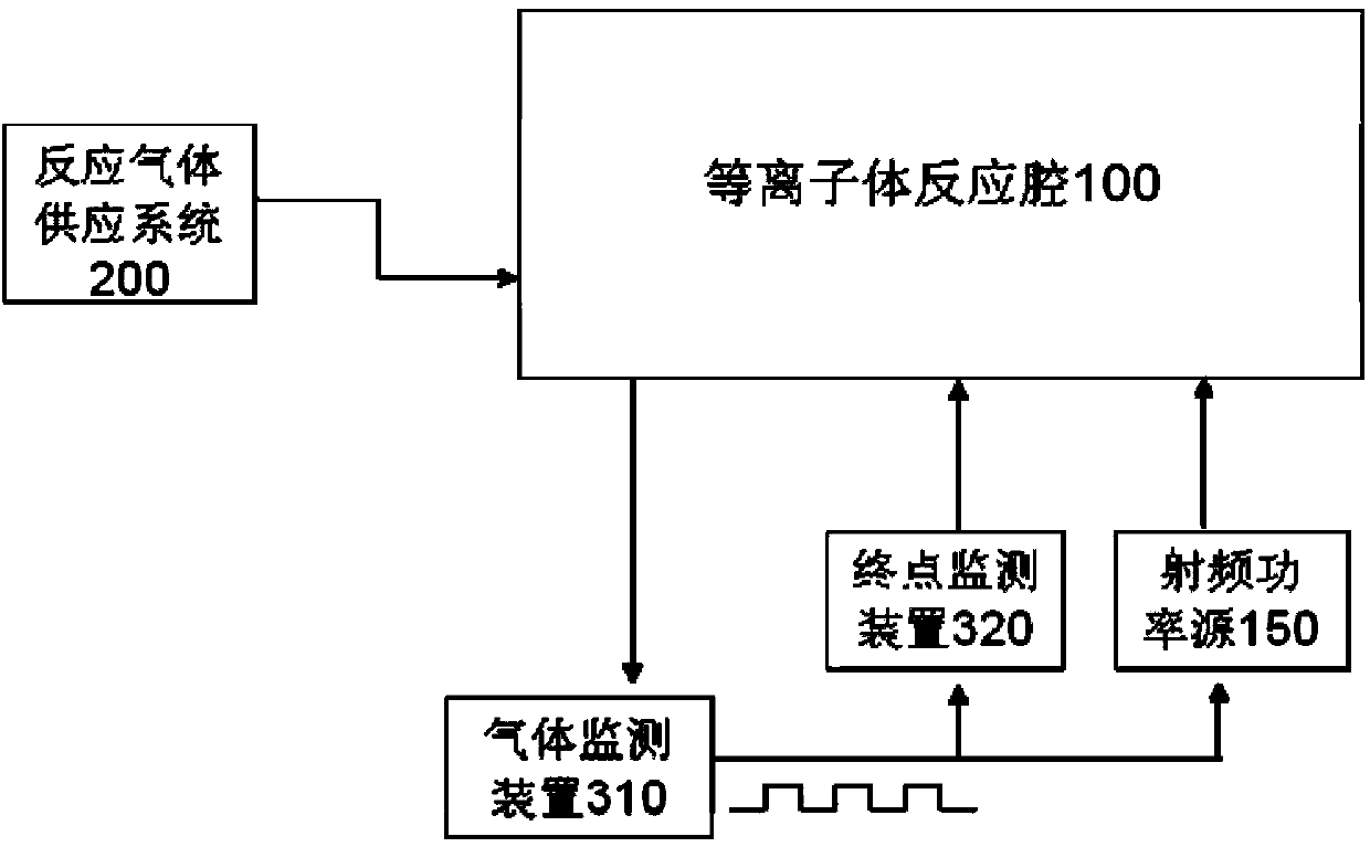
[0026] Such as figure 1 As shown, the present invention shows a system for improving the TSV etching process, including a plasma reaction chamber 100, the plasma reaction chamber 100 is connected to a reaction gas supply system 200 and a radio frequency power source 150, and the plasma reaction chamber 100 is also connected to a The gas monitoring device 310 and an endpoint monitoring device 320 are connected to the RF power source 150 and the endpoint monitoring device 320 and transmit synchronization signals to the RF power source 150 and the en...


PUM


Abstract

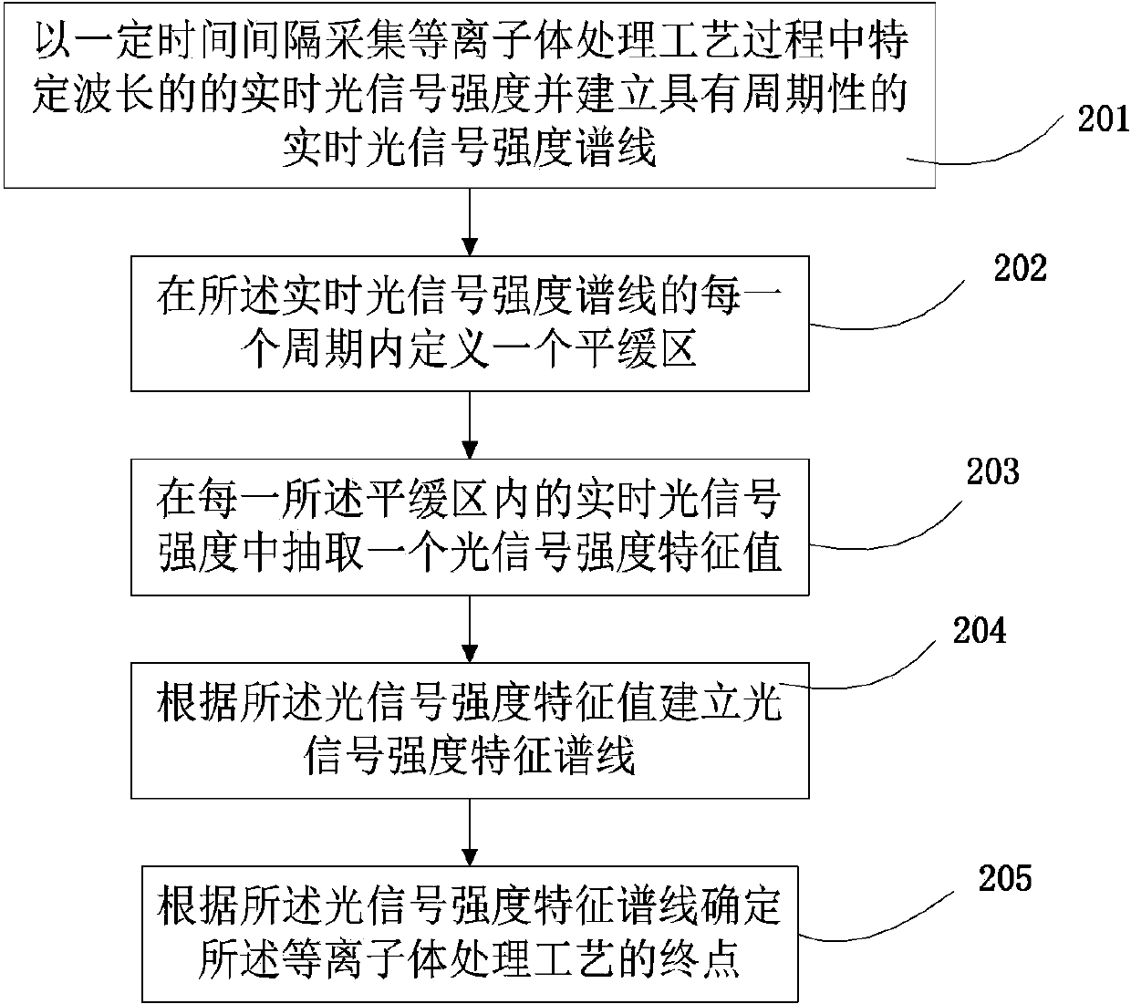
The invention discloses a system for improving TSV etching process and an etching endpoint monitoring method. A gas monitoring device is arranged outside a plasma reaction cavity, and the gas monitoring device is connected with a radio-frequency power source and an endpoint monitoring device, thereby realizing monitoring of the etching step and the depositing step of deep reaction plasma etching. The gas monitoring device determines the reaction gas on the surface of a substrate is an etching gas or a deposition gas by carrying out real-time monitoring on the spectrum emitted from the plasma on the surface of the substrate, and sends the results to the radio-frequency power source and the endpoint monitoring device so as to indicate the radio-frequency power source to output power matched with the gas, and meanwhile, to indicate the endpoint monitoring device to select some step to collect special-wavelength real-time light signal strength and establish a periodic real-time light signal strength spectral line, and the endpoint of the plasma processing process can be determined according to the light signal strength feature spectral line.

Description

Technical field [0001] The present invention relates to the technical field of semiconductor manufacturing, in particular to a system for improving TSV etching process and an etching endpoint monitoring method. Background technique [0002] In recent years, with the development of semiconductor manufacturing processes, the requirements for integration and performance of components have become higher and higher. Plasma Technology is playing a pivotal role in the field of semiconductor manufacturing. Plasma technology is used in many semiconductor processes, such as deposition processes (such as chemical vapor deposition), etching processes (such as dry etching), and the like, by exciting the plasma formed by the process gas. For the plasma treatment process, its accuracy is directly related to the feature size of the component. With the shrinking of the feature size of semiconductor devices and the rapid increase in the number and complexity of the plasma treatment process steps ...

Claims


Application Information

Patent Timeline
Patent Type & Authority Applications(China)
IPC IPC(8): H01L21/66
CPCH01L21/67253H01L22/26
Inventor 杨平黄智林
Owner ADVANCED MICRO FAB EQUIP INC CHINA
Learn More