

SOI LDMOS device with extending gate structure
A technology for extending gates and devices, applied in the field of semiconductor power devices, can solve problems such as uneven distribution of parasitic resistance and uneven temperature distribution, and achieve the effects of improving device withstand voltage, stable device operation, and uniform temperature distribution
- Summary
- Abstract
- Description
- Claims
- Application Information
AI Technical Summary
Problems solved by technology
Method used
Image

Examples
Embodiment 1
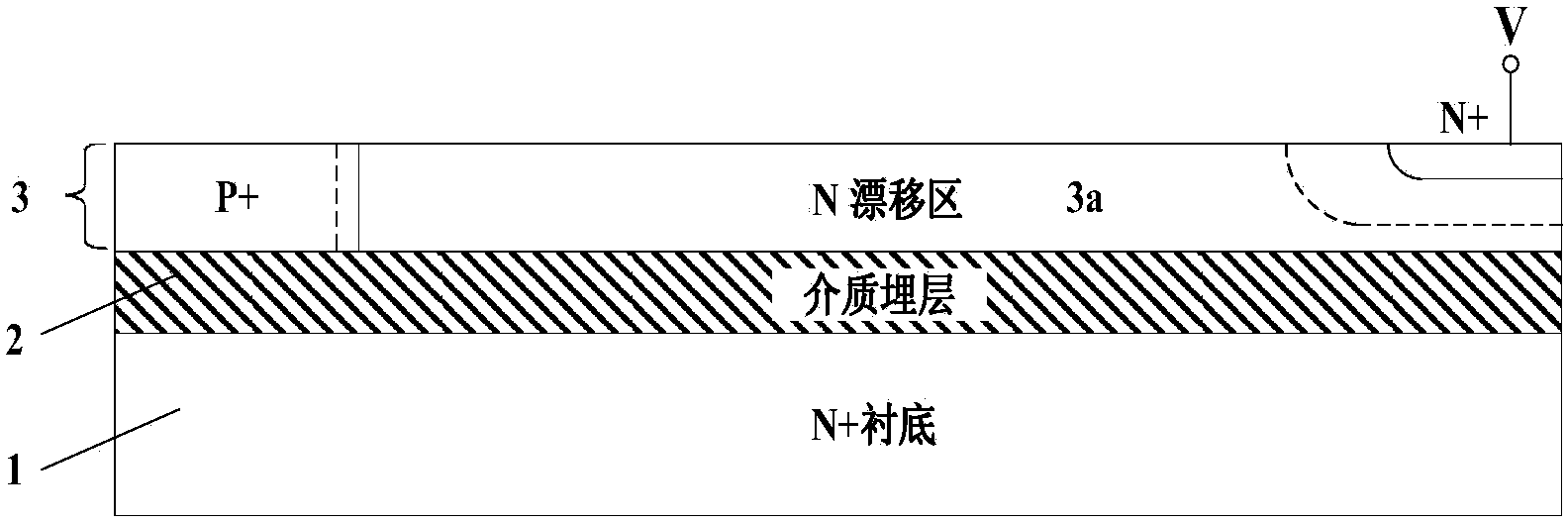
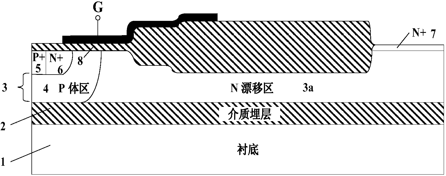
[0026] Figure 4a A cross-sectional view of a typical extended-gate SOI LDMOS device is given. It includes a substrate layer 1 vertically from bottom to top, a dielectric buried layer 2 and a first conductivity type semiconductor active layer 3 . One side of the first conductivity type semiconductor active layer 3 has a second conductivity type semiconductor body region 4, and the surface of the second conductivity type semiconductor body region 4 has an adjacent first conductivity type semiconductor source region 6 and a second conductivity type semiconductor body contact. Region 5, the first conductivity type semiconductor source region 6 and the second conductivity type semiconductor body contact region 5 lead out the terminal metallization source S; the other side of the first conductivity type semiconductor active layer 3 has a first conductivity type semiconductor drain Region 7, the surface of the drain region 7 of the semiconductor of the first conductivity type leads...
Embodiment 2
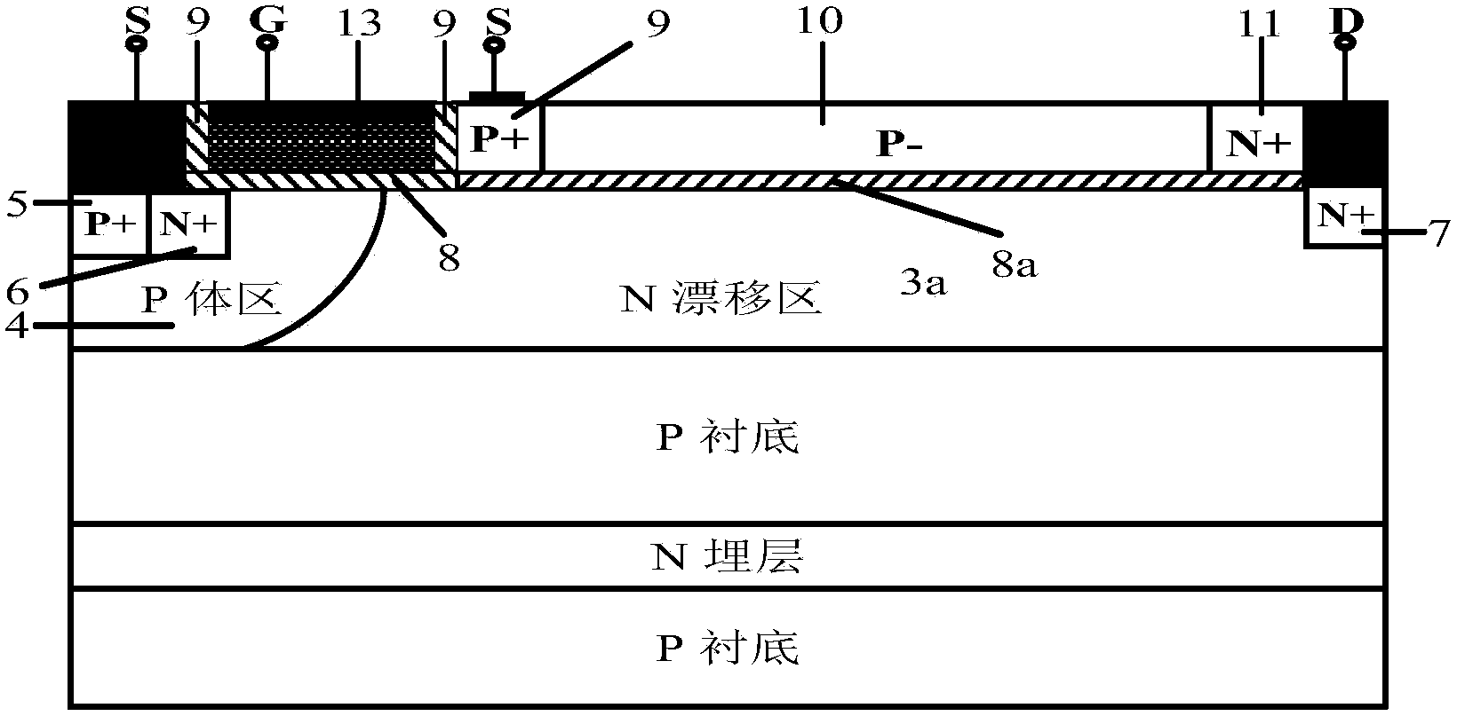
[0029] Figure 4b A schematic structure diagram of an extended-gate SOI LDMOS device with segmental change doping in the drift region is given. Compared with Embodiment 1, the doping concentration of the drift region 3a in the device of this embodiment increases in sections from near the body region 4 to near the drain region 7 . The sub-doped drift region will weaken the influence of the RESURF effect on the electric field distribution in the drift region in SOI devices. Therefore, compared with the device in Embodiment 1, the withstand voltage of the device in this example can be significantly improved, but since the drift region requires segmental doping, the process requirement is higher.
Embodiment 3
[0031] Figure 4c A schematic structure diagram of an extended-gate SOI LDMOS device doped with variable conductivity in the high-resistance region is given. Compared with Example 2, the device of this example adopts the doping of the second conductivity type in the part of the high resistance region 10 of the extended gate close to the gate contact region 9, and adopts the doping of the first conductivity type in the part close to the field stop region 11. Doped. The doping of the first conductivity type in the part close to the field stop region 11 can avoid damage to the drift region after the doping of the second conductivity type close to the field stop region 11 is fully depleted in the high resistance region 10 in the off-voltage withstand state of the device. Adverse effects of longitudinal electric field strength. Therefore, compared with the device in Embodiment 2, the withstand voltage of the device in this example will be improved, but because the doping type of ...
PUM
| Property | Measurement | Unit |
|---|---|---|
| Thickness | aaaaa | aaaaa |
Abstract
Description
Claims
Application Information