Method for realizing photoresist microstructure
A technology of microstructure and photoresist, which is applied in the field of photoresist microstructure and realizes the field of photoresist microstructure, which can solve the problems of leaving behind, difficult to popularize, and unable to develop the exposed area.
- Summary
- Abstract
- Description
- Claims
- Application Information
AI Technical Summary
Problems solved by technology
Method used
Image

Examples
Embodiment Construction
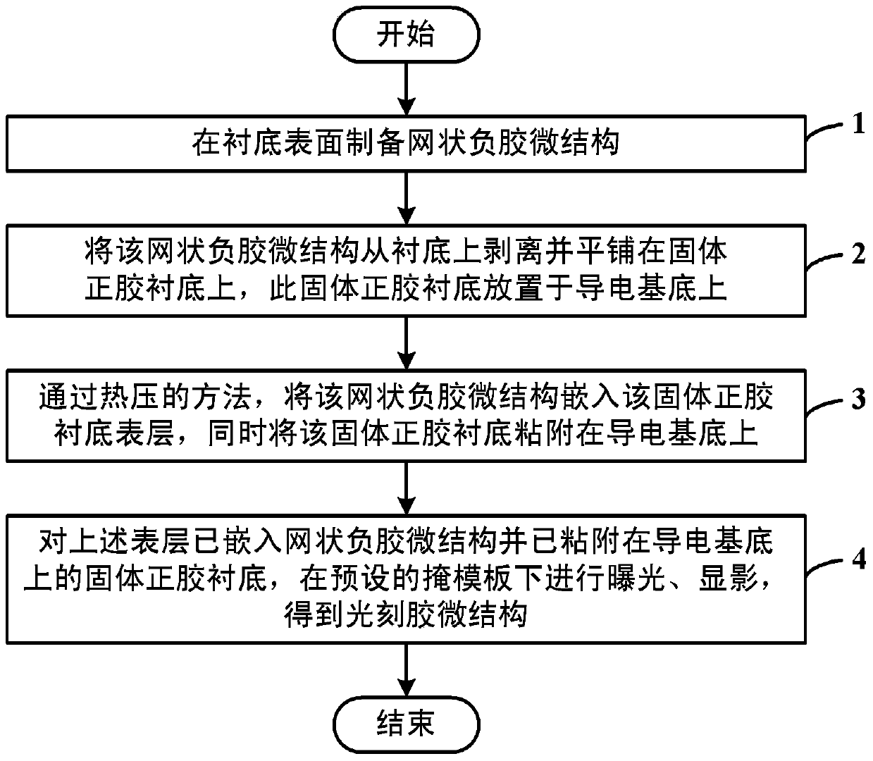
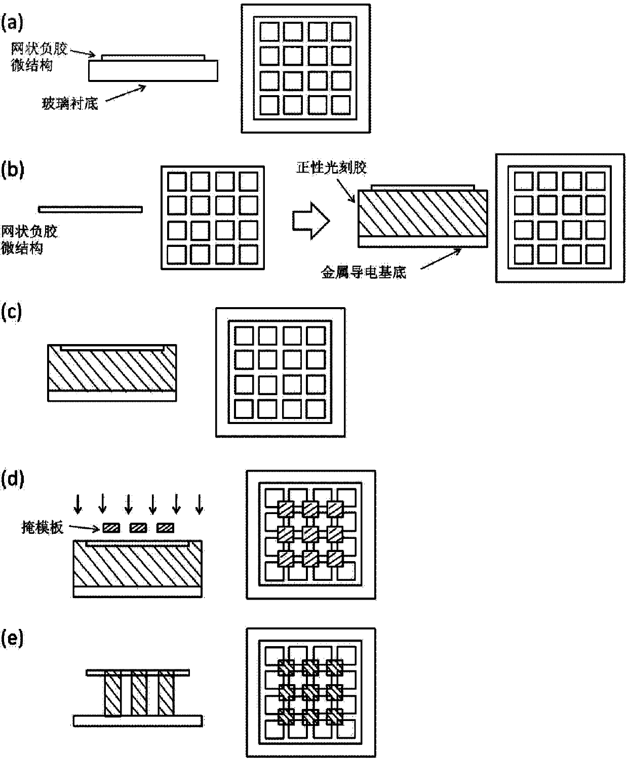
[0027] In order to make the object, technical solution and advantages of the present invention clearer, the present invention will be described in further detail below in conjunction with specific embodiments and with reference to the accompanying drawings.
[0028] First introduce the realization principle of the present invention below, the present invention can realize photoresist microstructure, especially have the photoresist microstructure of this feature of large aspect ratio, isolated microstructure array, its principle is as follows: When not using the present invention For the photoresist microstructure obtained after exposure and development, especially for a large aspect ratio and isolated microstructure array, desorption of the microstructure from the substrate or tilting and collapse of the microstructure usually occur. The physical reason for this phenomenon is the non-negligible force generated between the small-spaced microstructures caused by the flow impact o...
PUM
| Property | Measurement | Unit |
|---|---|---|
| Thickness | aaaaa | aaaaa |
Abstract
Description
Claims
Application Information
 - Generate Ideas
- Intellectual Property
- Life Sciences
- Materials
- Tech Scout
- Unparalleled Data Quality
- Higher Quality Content
- 60% Fewer Hallucinations
Browse by: Latest US Patents, China's latest patents, Technical Efficacy Thesaurus, Application Domain, Technology Topic, Popular Technical Reports.
© 2025 PatSnap. All rights reserved.Legal|Privacy policy|Modern Slavery Act Transparency Statement|Sitemap|About US| Contact US: help@patsnap.com