Core-shell field effect transistor and preparation method thereof

A field effect transistor and core source technology, applied in the field of gate-all-around field effect transistor and its preparation, can solve the problem of small driving current, and achieve the effects of increased mobility, good gate control capability and good modulation effect

Active Publication Date: 2014-12-10
PEKING UNIV
View PDF3 Cites 8 Cited by
  • Summary
  • Abstract
  • Description
  • Claims
  • Application Information

AI Technical Summary

Problems solved by technology

Traditional GAA devices also have the

Method used


Image

  • Core-shell field effect transistor and preparation method thereof
  • Core-shell field effect transistor and preparation method thereof
  • Core-shell field effect transistor and preparation method thereof

Examples


Embodiment Construction

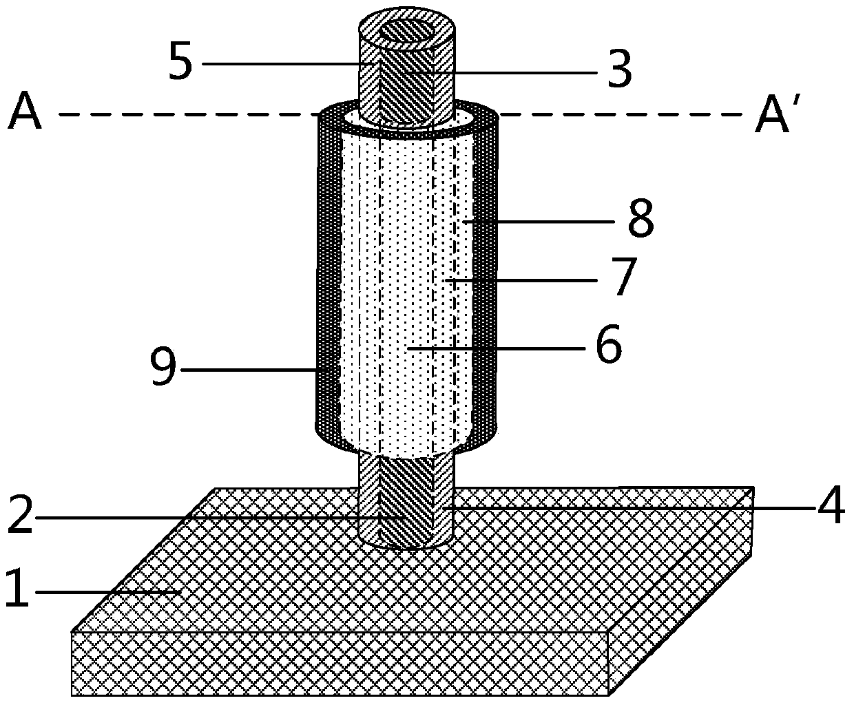
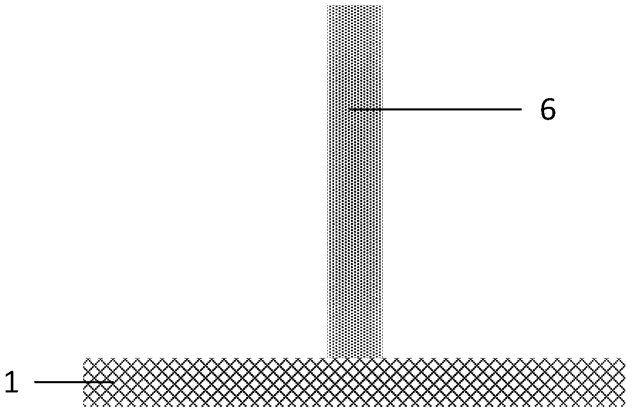
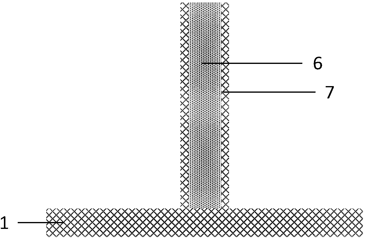
[0042]The present invention provides a gate-all-around field effect transistor combining a vertical channel, a core-shell structure and a junctionless structure, comprising a ring-shaped semiconductor core 6 in a vertical direction, a ring-shaped semiconductor shell 7 in a vertical direction, and a ring-shaped semiconductor shell 7 in a vertical direction. Gate electrode 9, a ring-shaped gate dielectric layer 8, a core source region 2, a core drain region 3, a shell source region 4, a shell drain region 5, and a semiconductor substrate 1; wherein, the core source region 2 is located vertically The bottom of the core channel 6 is connected to the substrate 1, the core drain region 3 is located on the top of the vertical core channel 6; the shell source region 4 is located at the bottom of the vertical shell channel 7, connected to the substrate 1, and the shell drain region 5 is located on the top of the vertical shell channel 7; the shell channel 7 surrounds the core channel 6 ...


PUM


Abstract

A surrounding gate field-effect transistor combined with a vertical channel, a core-casing structure and a junction-free structure comprises a surrounding semiconductor core in the vertical direction, a surrounding semiconductor casing in the vertical direction, a surrounding gate electrode, a surrounding gate dielectric layer, a core source region, a core drain region, a casing source region, a casing drain region and a semiconductor substrate, wherein the core source region is located at the bottom of a vertical core channel and connected with the substrate, and the core drain region is located at the top of the vertical core channel. The casing source region is located at the bottom of a vertical casing channel and connected with the substrate, and the casing drain region is located at the top of the vertical casing channel. The casing channel surrounds the core channel circularly. The gate dielectric layer surrounds the casing channel. The gate electrode surrounds the gate dielectric layer. The same impurities are doped into source and drain channels of the transistor, so that heat budget is greatly reduced, the impurity diffusion and abrupt junction forming problems are eliminated, process requirements are simplified, drive current is increased by utilizing a germanium core, integration machining photo-etching ultimate limit is broken through by utilizing the vertical channels and a surrounding gate structure, and the integration degree is improved.

Description

technical field [0001] The invention belongs to the field of field effect transistor logic devices and circuits in CMOS ultra large integrated circuits (ULSI), and in particular relates to a gate-ring field effect transistor combined with a vertical channel, a core-shell structure and a junctionless structure and a preparation method thereof. Background technique [0002] Driven by Moore's Law, the feature size of traditional MOSFETs has been shrinking, and now it has entered the nanometer scale. As a result, the negative effects of short-channel effects on devices have become more serious. The effects of leakage-induced barrier reduction and band-band tunneling increase the off-state leakage current of the device. In the research on new device structures, the source-drain doped Gate All Around transistor (GAA) structure is currently the most concerned one. GAA devices have better gate control characteristics, which can meet the sharpest characteristic requirements, so as t...

Claims


Application Information

Patent Timeline
IPC IPC(8): H01L29/78H01L29/423H01L29/06H01L29/10H01L21/336H01L21/28
CPCH01L29/1033H01L29/42392H01L29/66666
Inventor 孙雷徐浩张一博韩静文王漪张盛东
Owner PEKING UNIV
Why Eureka
Try Eureka