Fabrication method of high-precision multi-step microlens array

A technology of a microlens array and a manufacturing method, which is applied to the photoengraving process of lens and pattern surface, optics and other directions, can solve the problems of low yield and high requirements for production accuracy, and achieves high yield, low requirements for production accuracy and large size. economic effect

Active Publication Date: 2016-11-16
中航凯迈上海红外科技有限公司
View PDF5 Cites 0 Cited by
  • Summary
  • Abstract
  • Description
  • Claims
  • Application Information

AI Technical Summary

Problems solved by technology

[0007] The purpose of the present invention is to provide a new method for producing high-precision microlens arrays, which is used to solve the problems of high production precision requirements for operators and operating equipment and low yields in existing methods, and at the same time greatly saves Time to etch all steps

Method used


Image

  • Fabrication method of high-precision multi-step microlens array
  • Fabrication method of high-precision multi-step microlens array
  • Fabrication method of high-precision multi-step microlens array

Examples


Embodiment 2

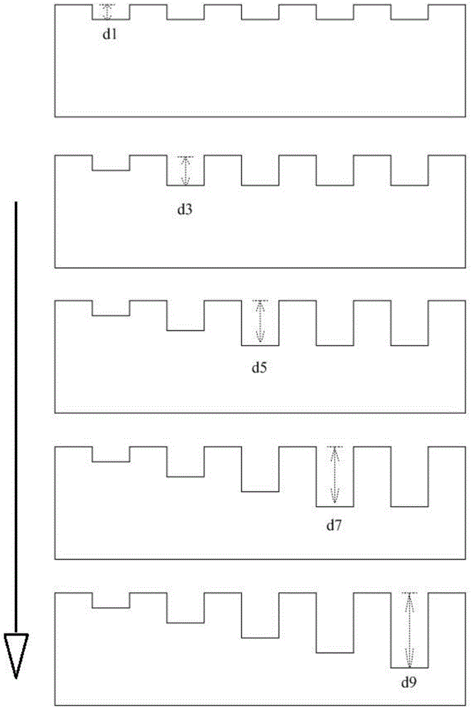
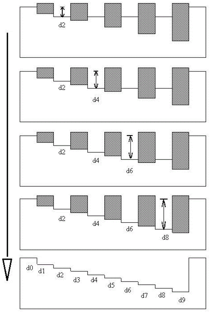
[0060] Figure 3 to Figure 5 It is a method for making four-step microlens arrays, and the depths of all the steps of the microlenses are d0, d1, d2, and d3; the specific steps are as follows:

[0061] 1), make the first set of steps set at intervals on the substrate, the steps are:

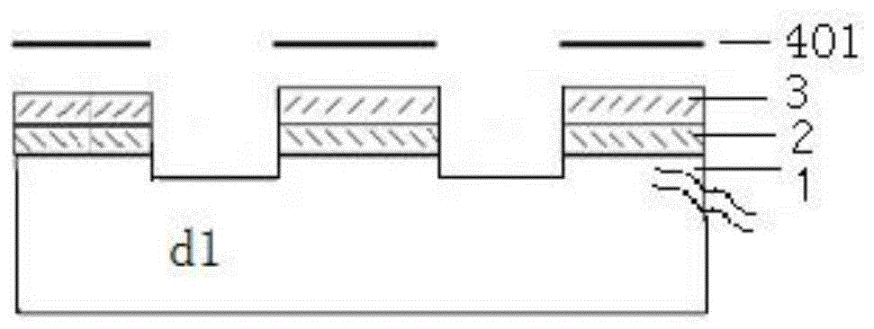
[0062] a), make a sacrificial layer and a positive photoresist layer on the substrate, perform photolithography and development by using a mask plate, and then etch two steps arranged at intervals and with a depth of d1; this step is as follows image 3 As shown, wherein the sacrificial layer is a negative photoresist layer, and the substrate can be a quartz material that is transparent to ultraviolet light, or a material such as silicon or germanium that is not transparent to ultraviolet light;

[0063] b), re-spin the positive photoresist, use the corresponding mask for photolithography and development, protect the step d1 that reaches the set depth, and further etch the remaining steps to for...

Embodiment 3

[0067] The difference from Example 2 is that, before etching the second set of steps, a mask protection layer is made by using the method of back exposure, such as Figure 8 Shown:

[0068] 1), make the first set of steps set at intervals on the substrate, the steps are:

[0069] a) Make a sacrificial layer and a positive photoresist layer on the substrate, and use a mask plate for photolithography, development and etching to etch two steps at intervals with a depth of d1; where the shielding layer 6 is the sacrificial The layer is an opaque chromium metal layer, and the base is quartz that can transmit ultraviolet light;

[0070] b), re-spin the positive photoresist, use the corresponding mask for photolithography, development and corrosion, protect the step with a set depth of d1, and further etch the remaining steps to form a step with a depth of d3 ;

[0071] 2), make a second set of steps between the first set of steps; the steps are:

[0072] c), apply negative photo...


PUM


Abstract

The invention relates to a method for manufacturing a high-precision multi-step microlens array. In the method, firstly, steps of an initial depth are made at equal intervals on a substrate; Etching is carried out to form steps with a set depth. This method not only requires relatively low manufacturing precision for operators and operating equipment, but also has a high yield rate, and can save a lot of etching time, which has great economic benefits.

Description

technical field [0001] The invention relates to a method for manufacturing a multi-step microlens array, which belongs to the field of photoelectric device manufacturing technology and micro-optics technology. Background technique [0002] The microlens array is an array composed of a series of tiny lenses with diameters of millimeters and micrometers in a certain arrangement. Micro-lenses and micro-lens arrays produced by micro-optical technology have become a new direction of scientific research and development due to their advantages of small size, light weight, easy integration, and arraying. [0003] With the rapid development of modern information technology, microlenses are widely used in various fields, such as copiers, image scanners, fax machines, cameras and medical and health equipment. The use of microlenses can gather light, improve the filling factor of the device, and solve the problems of optical crosstalk, low filling factor and decreased detection sensiti...

Claims


Application Information

Patent Timeline
Patent Type & Authority Patents(China)
IPC IPC(8): G02B3/00G02B27/44G03F7/00
Inventor 侯治锦司俊杰陈洪许吕衍秋王巍韩德宽
Owner 中航凯迈上海红外科技有限公司
Why Eureka
Try Eureka