Thin-film transistor, active matrix organic light-emitting diode assembly, and manufacturing method thereof

A technology of light-emitting diodes and thin-film transistors, which is applied in the direction of transistors, semiconductor devices, and electric solid-state devices. It can solve problems affecting the stability of OLEDs and changes in the voltage of storage capacitors, so as to avoid unstable or even failure of component operation and improve leakage current. Effect

Active Publication Date: 2014-12-24
EVERDISPLAY OPTRONICS (SHANGHAI) CO LTD
View PDF7 Cites 14 Cited by
  • Summary
  • Abstract
  • Description
  • Claims
  • Application Information

AI Technical Summary

Problems solved by technology

However, if Figure 1C As shown, when there is a leakage current in the switching transistor T1, the voltage of the storage capacitor will change, affecting the stability of the OLED

Method used


Image

  • Thin-film transistor, active matrix organic light-emitting diode assembly, and manufacturing method thereof
  • Thin-film transistor, active matrix organic light-emitting diode assembly, and manufacturing method thereof
  • Thin-film transistor, active matrix organic light-emitting diode assembly, and manufacturing method thereof

Examples


Embodiment approach

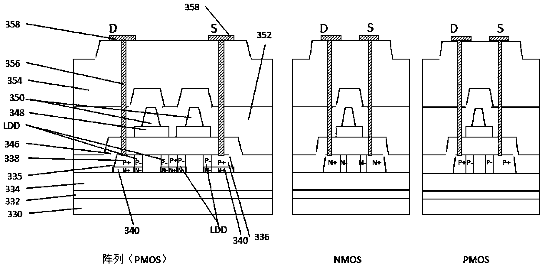
[0091] According to an exemplary embodiment, when the array substrate uses PMOS TFTs as switching elements, a P-N junction structure is formed in which the P+ region is on the upper layer and the N+ region is on the lower layer. It is easy to understand that when the array substrate uses NMOS TFTs as switching elements, the corresponding P-N junction structure can be formed, with the N+ region on the upper layer and the P+ region on the lower layer. In this way, the required depletion region structure can be obtained under the corresponding operating voltage.

[0092] According to the technical solution of the present disclosure, the leakage current of the switching thin film transistor in the AMOLED array substrate can be further improved, and the component operation instability or even failure caused by excessive leakage current can be avoided, thereby affecting the image quality of the display. It is easy to understand that the technical solutions according to the present d...


PUM


Abstract

The invention provides an active matrix organic light-emitting diode assembly which comprises a substrate and a plurality of pixels on the substrate. Each pixel at least comprises an organic light-emitting diode, a first thin-film transistor and a second thin-film transistor; wherein the second thin-film transistor is used for driving the organic light-emitting diode. The first thin-film transistor is used for driving the second thin-film transistor. The first thin-film transistor comprises the components of: a buffer layer on the substrate, a semiconductor layer on the buffer layer, a gate insulating layer which covers the semiconductor layer, and gate electrodes on the gate insulating layer. The semiconductor layer comprises a source area and a drain area in a first conductive type, and furthermore comprises a second conductive-type bottom doped area which is arranged at the bottom of the semiconductor layer and is below the source area and the drain area. Therefore, leakage current of an AMOLED assembly can be improved, thereby preventing assembly operation instability or failure caused by overlarge leakage current.

Description

technical field [0001] The present disclosure relates to active matrix organic light emitting displays, and in particular, to thin film transistors and active matrix organic light emitting diode (AMOLED) components including the thin film transistors and methods of manufacturing the same. Background technique [0002] Active Matrix Organic Light Emitting Diode (AMOLED) is a new generation of display technology, with self-illumination, wide viewing angle, high contrast, low power consumption, high response speed, high resolution, full color, thin Etc. AMOLED is expected to become one of the mainstream display technologies in the future. [0003] In the thin film transistor (TFT) array component part of the AMOLED, a low temperature polysilicon (LTPS: Low Temperature Poly Silicon) process is generally used. The quality of thin film transistors and array components including thin film transistors will also determine the final display quality of AMOLED. [0004] Figures 1A-1...

Claims


Application Information

Patent Timeline
Patent Type & Authority Applications(China)
IPC IPC(8): G09G3/32H01L29/786H01L29/06
CPCH01L29/78618H01L29/78621H01L27/1222H10K71/00
Inventor 许嘉哲黃家琦许民庆
Owner EVERDISPLAY OPTRONICS (SHANGHAI) CO LTD
Why Eureka
Try Eureka