Aluminum-free semiconductor laser structure

A technology of semiconductors and lasers, applied in the field of aluminum-free semiconductor laser structures, can solve problems such as limiting the maximum output power, achieve the effects of reducing strain, improving electro-optic conversion efficiency, and reducing voltage

Inactive Publication Date: 2014-12-24
TAIYUAN UNIV OF TECH
View PDF6 Cites 7 Cited by
  • Summary
  • Abstract
  • Description
  • Claims
  • Application Information

AI Technical Summary

Problems solved by technology

But the aluminum component material limits the maximum output power level of the structure

Method used


Image

  • Aluminum-free semiconductor laser structure

Examples


Embodiment Construction

[0035] The present invention will be further described below in conjunction with accompanying drawing:

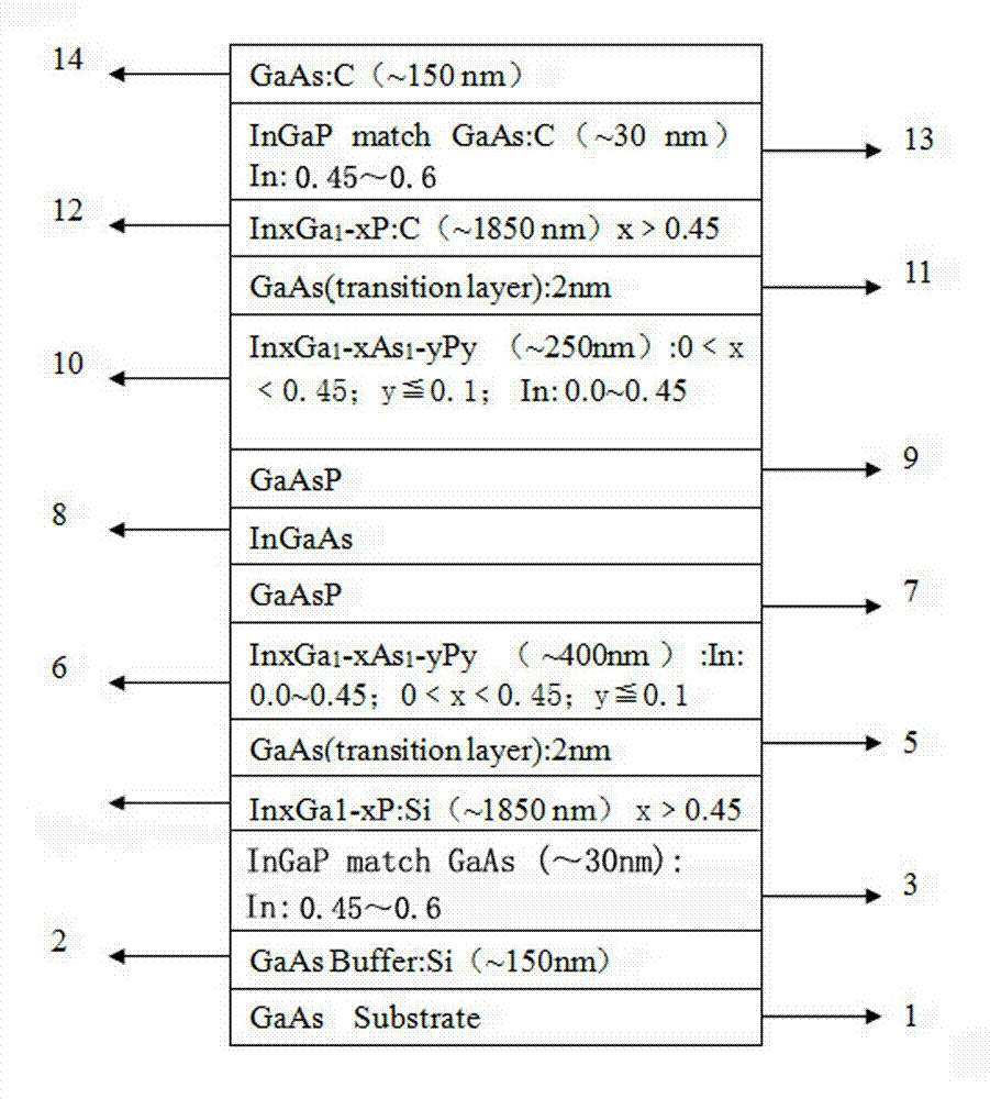
[0036] Such as figure 1 As shown, an aluminum-free semiconductor laser structure includes:

[0037] Substrate 1 is an N-type GaAs material of (100) plane;

[0038] The buffer layer 2 is set on the substrate 1 and is made of N-type GaAs material;

[0039] The lower matching layer 3 is set on the buffer layer 2 and is made of N-type InGaP material;

[0040] The lower confinement layer 4 is set on the lower matching layer 3 and is made of N-type InGaP material;

[0041] The lower transition layer 5 is set on the lower confinement layer 4 and is made of N-type GaAs material;

[0042] The lower waveguide layer 6 is set on the lower transition layer 5 and is made of N-type InGaAsP material;

[0043] The multi-quantum well layer is arranged on the lower waveguide layer 6, including the InGaAs potential well layer and the corresponding GaAsP barrier layer, and the number of pe...


PUM


Abstract

The invention belongs to the technical field of semiconductor optic electronics and particularly discloses an aluminum-free semiconductor laser structure. The aluminum-free semiconductor laser structure comprises a buffer layer, a lower matching layer, a lower limit layer, a lower transition layer, a lower waveguide layer, a multiple-quantum-well layer, an upper waveguide layer, an upper transition layer, an upper limit layer, an upper matching layer and an electrode contact layer, which epitaxially grow on a substrate from bottom to top by means of an organometallic chemical vapor deposition method. On the basis of asymmetric waveguide layers, how materials of the waveguide layers and the limit layers of a device influences mode limit factors, absorption loss, threshold current, output power, long service life and reliability is improved, so that a semiconductor layer of new structural system is obtained. The upper limit layer and the lower limit layer are made of InGap materials with small conduction-band difference, the upper waveguide layer and the lower waveguide layer are made of InGaAsP materials with small conduction-band difference and are of aluminum-free asymmetric straight waveguide structure.

Description

technical field [0001] The invention relates to the technical field of semiconductor lasers, in particular to an aluminum-free semiconductor laser structure. Background technique [0002] High-power semiconductor lasers have a very wide range of applications and market demands in the fields of pumping solid-state lasers and optical fiber lasers, medical fields and communication information fields. As the requirements for laser power become higher and higher, the problem of device reliability becomes more and more prominent. For high-power semiconductor lasers, the optical catastrophe damage on the cavity surface caused by high output optical power density and the temperature rise of the active region and cavity surface caused by various carrier recombination thermal effects become the limit of the maximum output optical power density, affecting A major factor in its reliability and longevity. [0003] With the development of laser technology and semiconductor film grow...

Claims


Application Information

Patent Timeline
Patent Type & Authority Applications(China)
IPC IPC(8): H01S5/343H01S5/20
Inventor 许并社董海亮梁建马淑芳余春艳
Owner TAIYUAN UNIV OF TECH
Why Eureka
Try Eureka