
Polyimide (PI) coating and baking method

A polyimide coating and baking method technology, applied in the field of MEMS, can solve problems such as irregular distribution, scrapped wafers, bad spots, etc., to reduce bubble defects, improve product yield and imaging quality, and reduce bubble defects. effect of the problem

Active Publication Date: 2015-01-07
北方广微科技有限公司
View PDF4 Cites 2 Cited by
  • Summary
  • Abstract
  • Description
  • Claims
  • Application Information

AI Technical Summary

Problems solved by technology

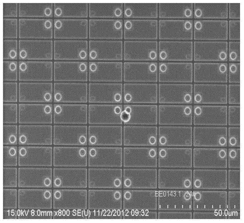
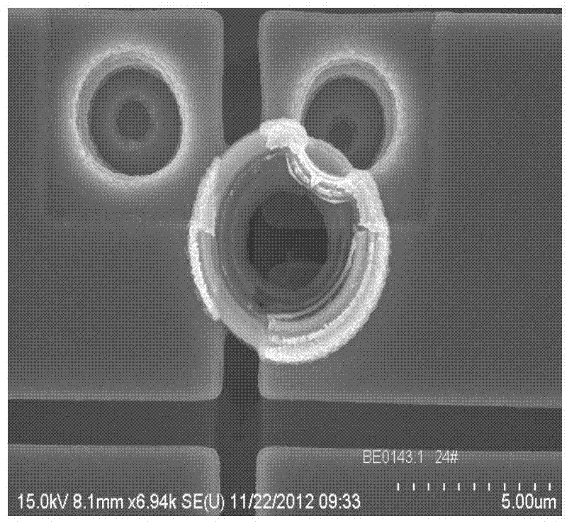
The distribution of bubble defects on the surface of the wafer is irregular. Once formed in the pixel area, because the bubble area loses the support of PI, fractures will be formed in the subsequent process, and bad spots will be formed directly, which will affect the imaging quality. Continuous distribution will even cause a film to be scrapped directly

Method used


Image

  • Polyimide (PI) coating and baking method
  • Polyimide (PI) coating and baking method
  • Polyimide (PI) coating and baking method

Examples


Embodiment Construction

[0048] Embodiments of the present invention are described in detail below.

[0049] Examples of the described embodiments are shown in the drawings, wherein like or similar reference numerals designate like or similar elements or elements having the same or similar functions throughout. The embodiments described below by referring to the figures are exemplary only for explaining the present invention and should not be construed as limiting the present invention. The following disclosure provides many different embodiments or examples for implementing different structures of the present invention. To simplify the disclosure of the present invention, components and arrangements of specific examples are described below. Of course, they are only examples and are not intended to limit the invention. Furthermore, the present invention may repeat reference numerals and / or letters in different instances. This repetition is for the purpose of simplicity and clarity and does not in i...


PUM


Abstract

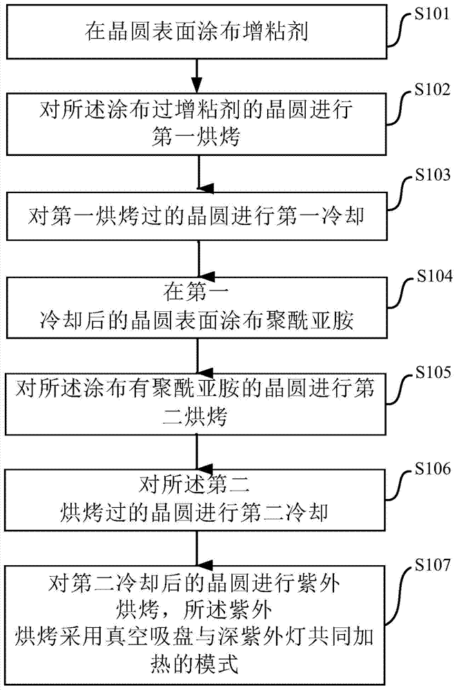
The invention provides a high-viscosity polyimide (PI) coating and baking method, which has the advantages of low cost and low defect density. The method comprises the following steps in sequence: coating the surface of a wafer with a tackifier; performing first baking on the wafer coated with the tackifier; performing first cooling on the wafer which is subjected to first baking; coating the surface of the wafer which is subjected to first cooling with PI; performing second baking on the wafer coated with the PI; performing second cooling on the wafer which is subjected to second baking; and performing ultraviolet baking on the wafer which is subjected to second cooling, wherein a common heating mode for heating through a vacuum sucking disk and a deep ultraviolet lamp is adopted in the ultraviolet baking. According to the embodiment of the invention, the problem of generation of bubble defect due to high viscosity of PI glue is solved, the product yield is increased, and the imaging quality is enhanced.

Description

technical field [0001] The invention relates to the technical field of MEMS, in particular to a polyimide coating and baking method with low cost and low defect density. Background technique [0002] MEMS (Micro Electro Mechanical System) is an advanced manufacturing technology platform. It is developed on the basis of semiconductor manufacturing technology. MEMS technology adopts a series of existing technologies and materials such as photolithography, corrosion, and thin film in semiconductor technology. Infrared sensors with superior performance can be manufactured using advanced MEMS micromachining technology. Today, infrared sensors are used more and more widely, such as non-contact rapid measurement of body temperature in medicine, which is of great significance in the need to measure the temperature of a large number of people; in addition, it is also used in scientific research and military, such as Infrared spectrometer, missile guidance, thermal imaging, laser d...

Claims


Application Information

Patent Timeline
IPC IPC(8): B81C1/00B05D1/38B05D3/02B05D3/00B05C11/02
Inventor 高江雷述宇
Owner 北方广微科技有限公司
Learn More