Transistor with high electronic mobility

A high electron mobility, transistor technology, used in circuits, electrical components, semiconductor devices, etc., can solve the problems of high activation energy, reduced device performance, low hole concentration, etc., to improve the breakdown voltage and improve the concentration effect. Effect

Active Publication Date: 2015-01-07
GPOWER SEMICON
View PDF8 Cites 16 Cited by
  • Summary
  • Abstract
  • Description
  • Claims
  • Application Information

AI Technical Summary

Problems solved by technology

At the same time, Mg is generally used for p-type doping of GaN, and the activation energy of Mg is high, resulting in low doping efficiency, low hole concentration, and Mg has a serious memory effect, and diffusion into the barrier layer will also reduce the device performance. performance
Therefore, it is more difficult to apply the traditional field limit ring structure and technology in GaN-based HEMTs.

Method used


Image

  • Transistor with high electronic mobility
  • Transistor with high electronic mobility
  • Transistor with high electronic mobility

Examples


Embodiment 1

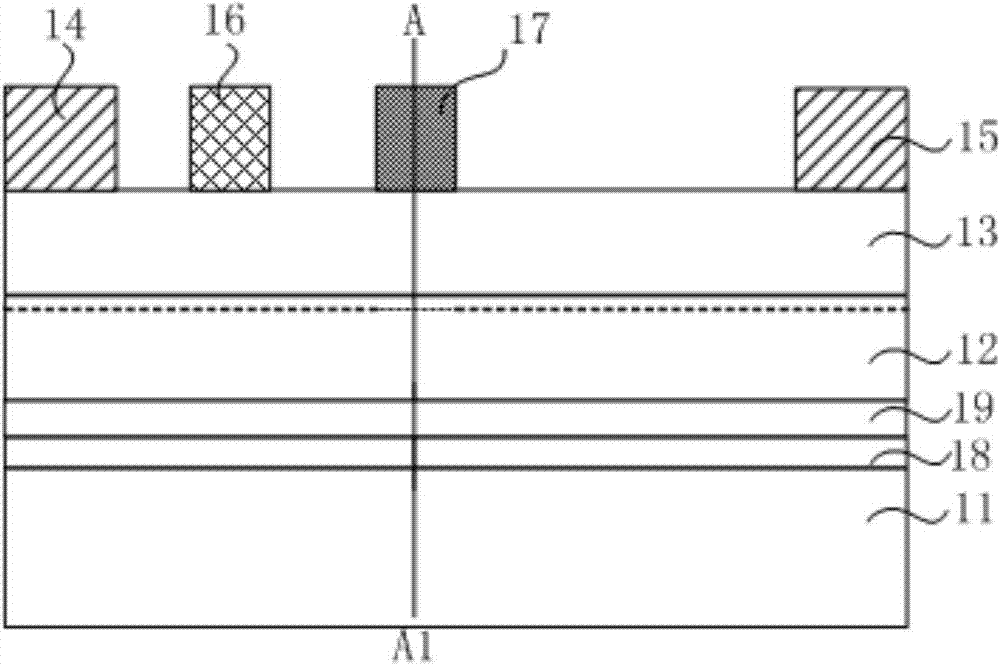
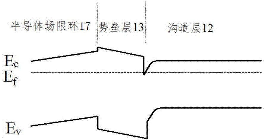
[0039] figure 1 is a structural diagram of a high electron mobility transistor provided in Embodiment 1 of the present invention, figure 2 It is a high electron mobility transistor provided by Embodiment 1 of the present invention. figure 1 The energy band diagram in the direction of AA1, now combined with figure 1 and figure 2 Embodiment 1 of the present invention will be described.

[0040] See figure 1 , the high electron mobility transistor includes a substrate 11, a channel layer 12 on the substrate 11, a barrier layer 13 on the channel layer 12, a source 14 on the barrier layer 13, and a drain 15 And a Schottky gate 16 located between the source 14 and the drain 15 , and a semiconductor field confining ring 17 located between the Schottky gate 16 and the drain 15 on the barrier layer 13 .

[0041] In this embodiment, the material of the substrate 11 may be gallium nitride, silicon, sapphire, silicon carbide, aluminum nitride or other semiconductor materials.

[0...

Embodiment 2

[0059] Figure 4 It is a structural diagram of a high electron mobility transistor provided in Embodiment 2 of the present invention, please refer to Figure 4 , the high electron mobility transistor comprises a substrate 11, a nucleation layer 18 on the substrate 11, a buffer layer 19 on the nucleation layer 18, a channel layer 12 on the buffer layer 19, a channel layer on the The barrier layer 13 on the barrier layer 12, the source 14 on the barrier layer 13, the drain 15 and the Schottky gate 16 between the source 14 and the drain 15, the Schottky gate 16 on the barrier layer 13 At least two semiconductor field confining rings between the base gate 16 and the drain 15 .

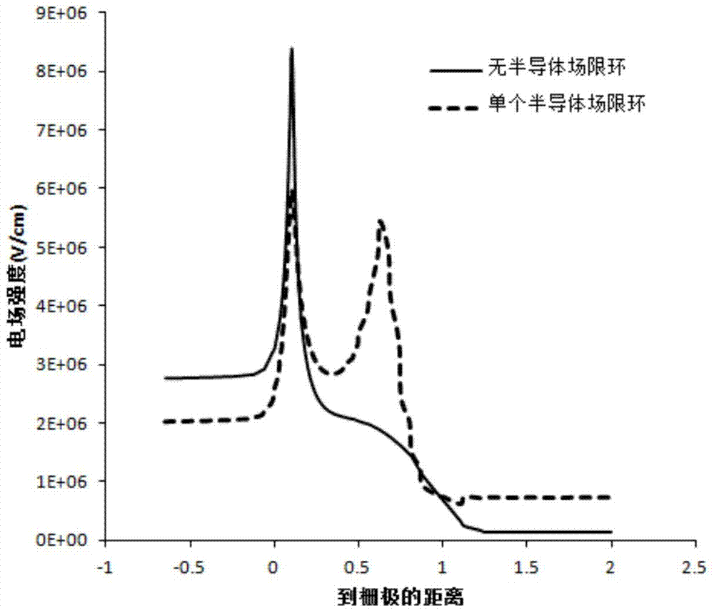
[0060] The second embodiment is based on the first embodiment above, and the difference from the first embodiment is that the high electron mobility transistor provided by the second embodiment includes a Schottky gate 16 and a drain 15 on the barrier layer 13 There are at least two semiconductor field con...

Embodiment 3

[0067] Figure 5 It is a structural diagram of a high electron mobility transistor provided in Embodiment 3 of the present invention, please refer to Figure 5 , the high electron mobility transistor comprises a substrate 11, a nucleation layer 18 on the substrate 11, a buffer layer 19 on the nucleation layer 18, a channel layer 12 on the buffer layer 19, a channel layer on the The barrier layer 13 on the barrier layer 12, the source 14 on the barrier layer 13, the drain 15 and the Schottky gate 16 between the source 14 and the drain 15, the Schottky gate 16 on the barrier layer 13 At least two semiconductor field confinement rings between the base gate 16 and the drain 15, the composition of the at least two semiconductor field confinement rings is uniform, and the thickness of the at least two semiconductor field confinement rings is close to the Schottky gate The electrode 16 gradually decreases towards the drain electrode 15.

[0068] In this embodiment, the present inve...


PUM


Abstract

The invention discloses a transistor with high electronic mobility. The transistor with the high electronic mobility comprises a substrate, a channel layer, a barrier layer, a source electrode, a drain electrode, a schottky grid electrode and at least one semiconductor field limiting ring, wherein the channel layer is located on the substrate, the barrier layer is located on the channel layer, the source electrode and the drain electrode are located on the barrier layer, the schottky grid electrode is located between the source electrode and the drain electrode, and the semiconductor field limiting rings are located at the position, between the schottky grid electrode and the drain electrode, on the barrier layer. According to the transistor with the high electronic mobility, the concentration of two-dimensional electron gas on the interface between the barrier layer and the channel layer can be adjusted, the concentration effect of an electric field on a grid electrode edge can be improved effectively, and the breakdown voltage of the transistor with the high electronic mobility is increased.

Description

technical field [0001] The invention relates to the technical field of semiconductors, in particular to a high electron mobility transistor. Background technique [0002] GaN-based high electron mobility transistor (High Electron Mobility Transistor, referred to as HEMT) has a high two-dimensional electron gas concentration (Two Dimensional Electron Gas, referred to as 2DEG) and a large breakdown voltage, which has attracted extensive attention from scientific research institutions and enterprises. Making the breakdown voltage as high as possible while maintaining low on-resistance is one of the biggest challenges in current GaN-based HEMT research. [0003] GaN HEMT devices usually have a planar structure. When the HEMT is in the off state, a negative bias is applied to the gate, a positive bias is applied to the drain, and the source is grounded, which will cause electric field lines to gather at the edge of the gate near the drain. , an electric field spike is formed. G...

Claims


Application Information

Patent Timeline
Patent Type & Authority Applications(China)
IPC IPC(8): H01L29/778
CPCH01L29/0603H01L29/778H01L29/0611H01L29/0657H01L29/2003H01L29/66462H01L29/7786H01L29/0607H01L29/404H01L29/47
Inventor 裴轶
Owner GPOWER SEMICON
Why Eureka
Try Eureka