Preparation method of vertical structure LED thin film chip capable of releasing stress

A vertical structure, thin-film chip technology, applied in the direction of electrical components, circuits, semiconductor devices, etc., can solve the problems of chip displacement, device lithography difficulty, single chip bulging, etc., to release residual stress, improve photoelectric performance, reduce The effect of production costs

Active Publication Date: 2017-06-16
NANCHANG UNIV +1
View PDF2 Cites 0 Cited by
  • Summary
  • Abstract
  • Description
  • Claims
  • Application Information

AI Technical Summary

Problems solved by technology

The CN201110026143 patent adopts the method of multiple transfers to release the stress. This method of multiple transfers can indeed fully release the stress, but it brings some new problems, such as: the problem of chip displacement (resulting in the difficulty of complete alignment of subsequent device lithography, etc. ) and single chip bulging (leading to cracks in the subsequent process of the chip), which will affect the yield and reliability of the chip

Method used


Image

  • Preparation method of vertical structure LED thin film chip capable of releasing stress
  • Preparation method of vertical structure LED thin film chip capable of releasing stress
  • Preparation method of vertical structure LED thin film chip capable of releasing stress

Examples


Embodiment 1

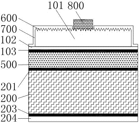
[0048] (1), such as figure 2As shown, a substrate 100 is provided on which an LED thin film 101 is grown, wherein the LED thin film 101 includes a buffer layer, an n-type layer, a light emitting layer and a p-type layer. Preferably, the material of the substrate 100 is Si, and the LED thin film 101 is an AlGaInN thin film grown by MOCVD. In other embodiments of the present invention, the substrate 100 can also be any one of sapphire, SiC, GaN, GaAs or AlN, and the LED thin film 101 is not limited to AlGaInN thin film, and can also be other Semiconductor thin films that require stress release, such as aluminum gallium indium phosphide epitaxial films on gallium arsenide substrates.

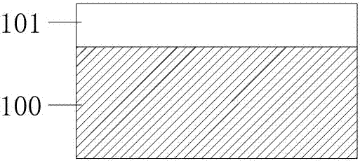
[0049] (2), such as image 3 As shown, a reflective contact layer 102 , a barrier layer 103 and a first bonding layer 104 are sequentially formed on the LED film 101 by electron beam evaporation. The reflective contact layer 102 has good ohmic contact performance with the GaN-based LED thin fil...


PUM


Abstract

The invention discloses a method for preparing a perpendicular structure LED thin film chip capable of releasing stress and a structure. On the basis that materials of a barrier layer, especially a first bonding layer, a middle layer and a second bonding layer and the structure are scientifically selected and designed, it is designed that metal or alloy between an LED thin film and a base board is melted or partially melted through low-temperature annealing treatment after a substrate is removed so that the LED thin film can freely extend and be automatically flatted in the melting process, the effect of effectively releasing the residual stress in the LED thin film is achieved, and the photoelectric property of the LED chip can be prevented from being damaged when the annealing and melting temperature is too high. The structure comprises the substrate, wherein the LED thin film internally provided with a buffering layer, an n-type layer, a luminous layer and a P-type layer is arranged on the substrate, and a reflecting contact layer and the barrier layer are deposited on the LED thin film in sequence. The structure is characterized in that a mixed layer is formed below the barrier layer, and a base board front face protection layer, the base board, a base board reverse side protection layer and the contact layer are arranged below the mixed layer.

Description

technical field [0001] The invention belongs to the technical field of semiconductor optoelectronic device manufacturing, and in particular relates to a preparation method and structure of a vertical structure LED thin film chip capable of releasing stress. Background technique [0002] As a new generation of green solid light source, LED (Light Emitting Diode) is an ideal energy-saving and environmentally friendly product, suitable for status indication, traffic lights, large-screen display, lighting and other places. GaN-based LEDs are gradually entering thousands of households. [0003] From the structure of LED, GaN-based LED can be divided into front structure, flip structure and vertical structure. The traditional front-mounted structure LED has big problems in chip light emission and heat dissipation, and there is a phenomenon of current congestion, which limits the further improvement of its luminous efficiency and reliability, and is difficult to meet the needs of ...

Claims


Application Information

Patent Timeline
Patent Type & Authority Patents(China)
IPC IPC(8): H01L33/00H01L33/12
CPCH01L33/005H01L33/12H01L2933/0008
Inventor 刘军林王光绪汤英文熊传兵江风益
Owner NANCHANG UNIV
Why Eureka
Try Eureka