Method for forming semiconductor device and method for forming fin field effect transistor

A fin field effect, semiconductor technology, applied in the direction of semiconductor devices, semiconductor/solid-state device manufacturing, electrical components, etc., can solve the problems of large height drop, affecting the performance of semiconductor devices, affecting the manufacturing process of semiconductor devices, etc., to achieve improved performance. Effect

Active Publication Date: 2015-01-14
SEMICON MFG INT (SHANGHAI) CORP
View PDF6 Cites 5 Cited by
  • Summary
  • Abstract
  • Description
  • Claims
  • Application Information

AI Technical Summary

Problems solved by technology

[0008] Currently, in the manufacturing process of FinFET, after the gate material layer 4 undergoes the grinding process, various parts of the surface 41 have large unevenness defects, and the height difference is large. This defect directly affects the subsequent semiconductor device manufacturing process, and affects the final The performance of the formed semiconductor device

Method used


Image

  • Method for forming semiconductor device and method for forming fin field effect transistor
  • Method for forming semiconductor device and method for forming fin field effect transistor
  • Method for forming semiconductor device and method for forming fin field effect transistor

Examples


Embodiment Construction

[0045] As described in the background art, during the preparation of fin-type field effect transistors, the surface of the gate material after the grinding layer process will have a large range of uneven defects, which will affect the subsequent preparation process of the semiconductor device and the final semiconductor device. Performance.

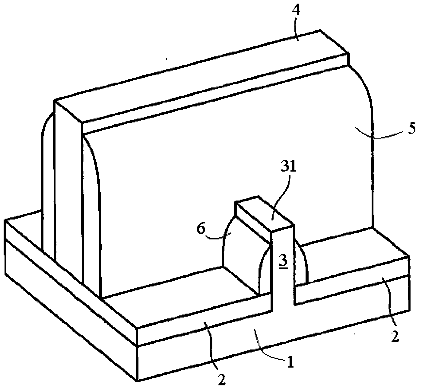
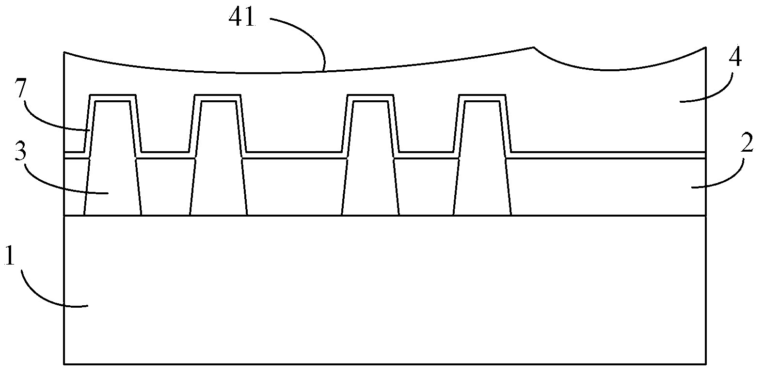
[0046] The reason for this defect may be, refer to figure 2 As shown, the fin 3 protrudes on the surface of the semiconductor substrate 1, so the semiconductor material layer formed on the semiconductor substrate 1 has obvious protruding parts before grinding (refer to image 3 The protrusion 150 of the semiconductor material layer 140 in the fin-type field-effect transistor is often formed on a semiconductor substrate at the same time during the preparation of the fin-type field-effect transistor. Based on the special structure of the fin 3 and the semiconductor The density of the arrangement of the fins 3 on the substrate 1 is different, a...


PUM


Abstract

The invention provides a method for forming a semiconductor device and a method for forming a fin field effect transistor. According to the method for forming the semiconductor device, the position on the surface of a semiconductor material layer at a device dense area of a semiconductor substrate is higher than the position of a semiconductor material layer at a device sparse area, hence, the semiconductor material layer at the device sparse area is covered with a mask layer, ions are injected to the partial thickness part of the semiconductor material layer at the dense area, so that an ion injection area is formed, and then the ion injection area is removed. After the ions are injected, the characteristic of a semiconductor material in the ion injection area is changed, the character of the ion injection area of the semiconductor material layer differs from the character of a nonionic injection area of the semiconductor material layer, the semiconductor material layer with the nonionic injection area is hardly affected in the subsequent removing process of the ion injection area, accordingly, the heights of the semiconductor material layers at the device sparse area and the device dense area are close to be the same ultimately, and therefore the performance of the semiconductor device is improved.

Description

Technical field [0001] The invention relates to the field of semiconductor formation, in particular to a method for forming a semiconductor device and a method for forming a fin field effect transistor. Background technique [0002] With the rapid development of integrated circuit (IC) manufacturing technology, especially after entering the field of submicron feature size, the size of traditional integrated circuits is shrinking, and the size of semiconductor components must be correspondingly smaller. [0003] However, for example, a MOS transistor generates a switching signal by applying a voltage to the gate and adjusting the current through the channel region. However, when semiconductor technology enters the node below 45 nanometers, the traditional planar MOS transistor has a weaker ability to control the channel current. , Causing serious leakage current. Conventional MOS transistors can no longer meet the requirements for device performance, and multi-gate devices have rec...

Claims


Application Information

Patent Timeline
Patent Type & Authority Applications(China)
IPC IPC(8): H01L21/336H01L29/78
CPCH01L29/66795
Inventor 程继邓武锋
Owner SEMICON MFG INT (SHANGHAI) CORP
Why Eureka
Try Eureka