

Multilayer film improving extreme ultraviolet spectral purity and oxidation resistance
A spectral purification layer and anti-oxidation technology, applied in the field of multilayer films, can solve the problems of easy occurrence of oxide layer and carbon pollution deposition layer, pollution oxide layer, affecting the inhibition effect of spectral purification layer, etc., so as to improve the imaging quality and use Longevity, the effect of improving spectral purity
- Summary
- Abstract
- Description
- Claims
- Application Information
AI Technical Summary
Problems solved by technology
Method used
Image

Examples
Embodiment 1
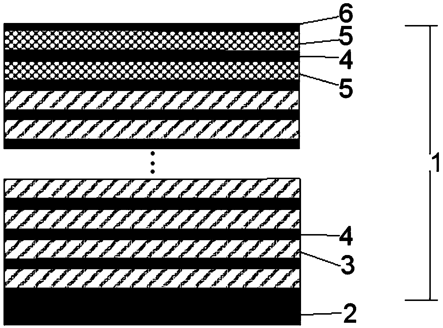
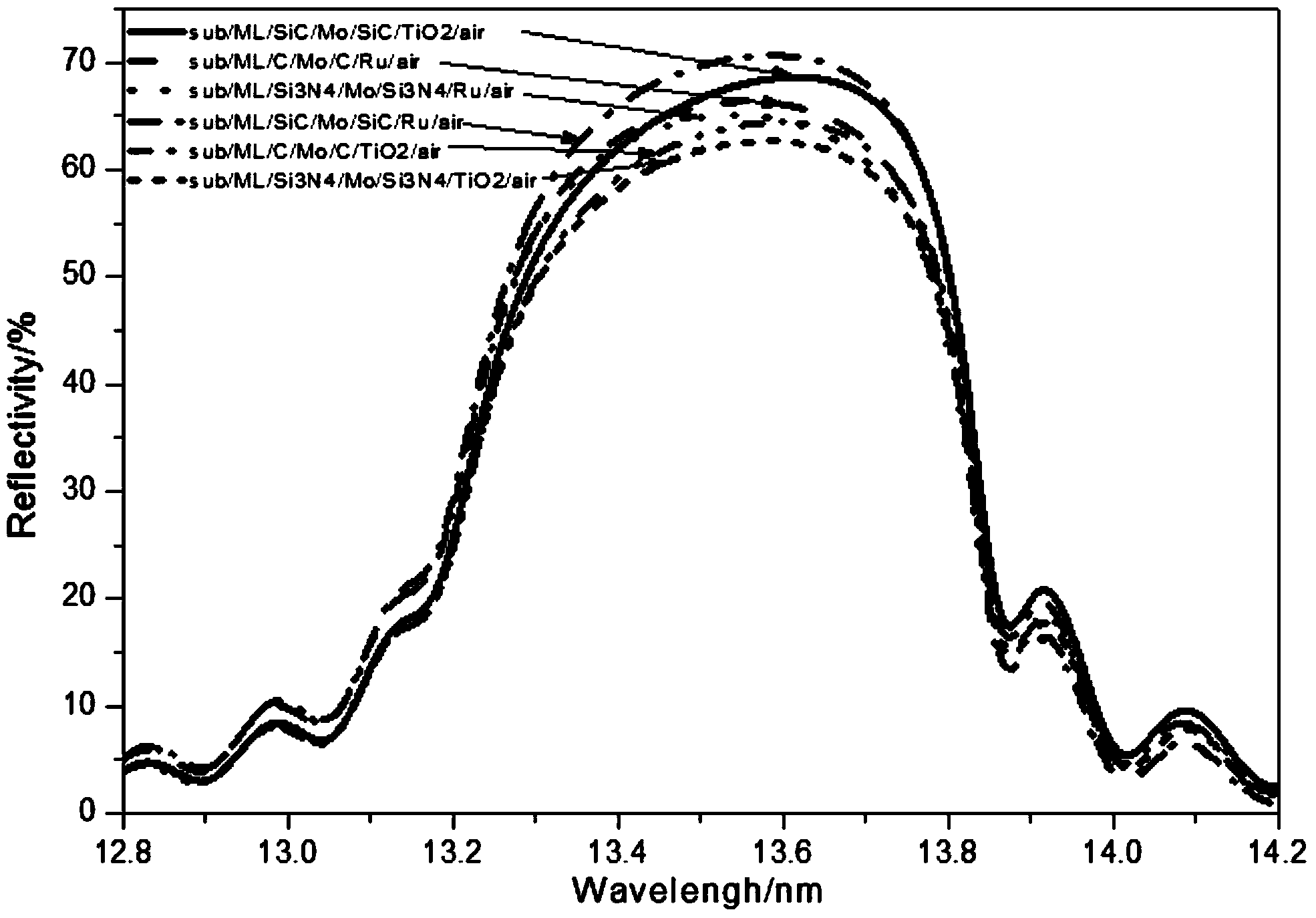
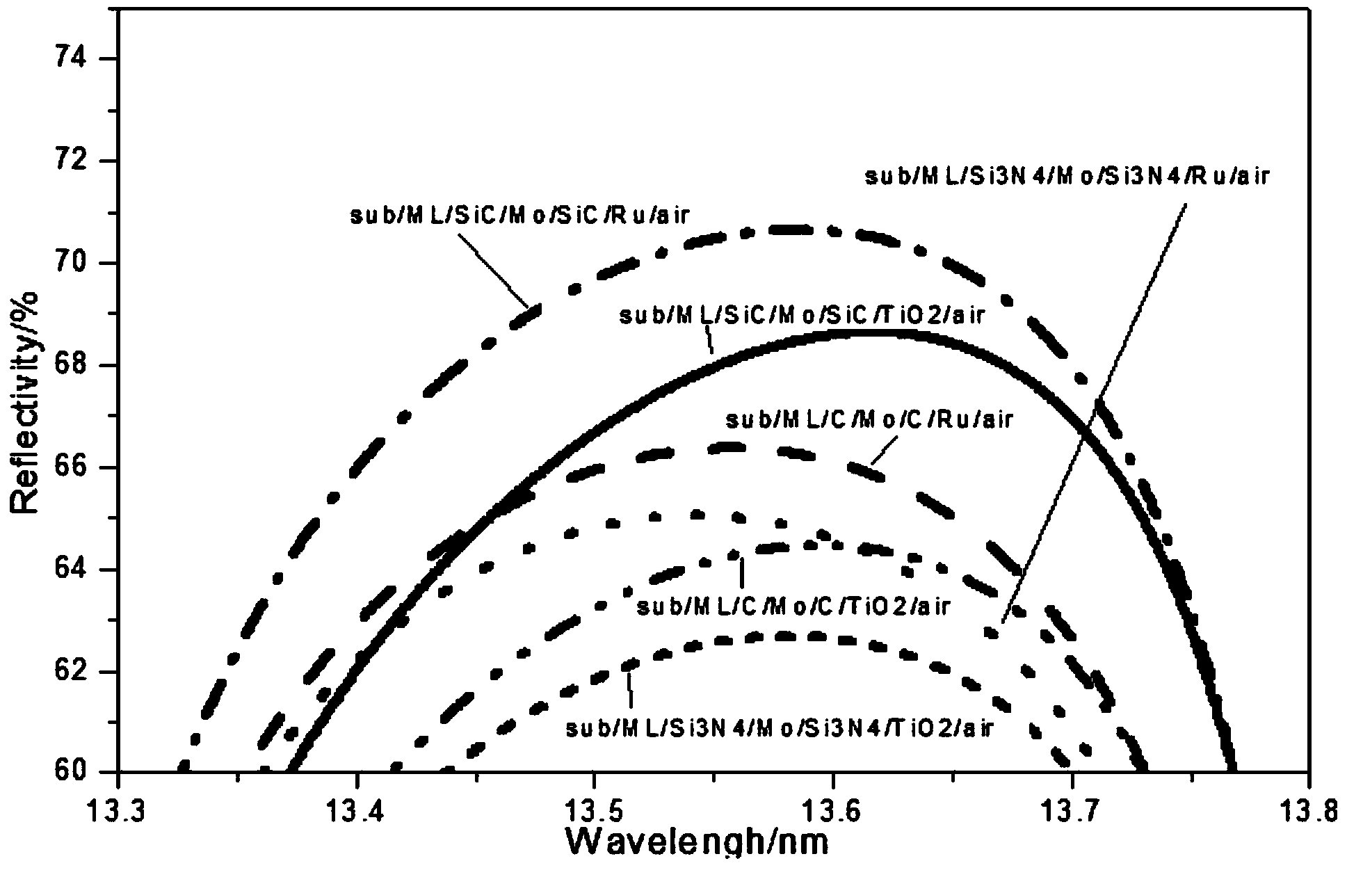
[0036] Such as figure 1 As shown, the structure of the multilayer film 1 is composed of 40 cycles of Si layer 3 / Mo layer 4, spectral purification layer 5, Mo layer 4, spectral purification layer 5 and protective layer 6. The multilayer film 1 is disposed on the substrate 2, wherein the corresponding Si layer 3 and the corresponding Mo layer 4 constitute a period, and the period thickness is 7 nm. The thickness of each spectral purification layer 5 is 3 nm, and the material is C material. The thickness of the uppermost protective layer 6 is 2 nm, and the material is Ru. Because the existence of the spectral purification layer 5 will make the multilayer film 1 less reduce the reflectance at 13.5nm, its out-of-band band, especially 160nm ~ 240nm, will have an effective inhibitory effect on the reflectivity; Layer 6 effectively reduces the oxidation of the upper film. Applying the multilayer film 1 to the substrate 2 is preferably a magnetron sputtering technology, where the Si...
Embodiment 2
[0038] The structure of the multilayer film 1 is composed of 40 cycles of Si layer 3 / Mo layer 4, spectral purification layer 5, Mo layer 4, spectral purification layer 5 and protective layer 6. The multilayer film 1 is disposed on the substrate 2, wherein the corresponding Si layer 3 and the corresponding Mo layer 4 constitute a period, and the period thickness is 7 nm. The thickness of each spectral purification layer 5 is 5 nm, and the material is SiC. The thickness of the uppermost protective layer is 1nm, the material is TiO 2 . Because the existence of the spectral purification layer 5 will make the multilayer film 1 less reduce the reflectance at 13.5nm, its out-of-band band, especially 160nm ~ 240nm, will have an effective inhibitory effect on the reflectivity; Layer 6 effectively reduces the oxidation of the upper film. Applying the multilayer film 1 to the substrate 2 is preferably a magnetron sputtering technology, where the Si layer 3 and the Mo layer 4 are DC ma...
Embodiment 3
[0040] The structure of the multilayer film 1 is composed of 40 cycles of Si layer 3 / Mo layer 4, spectral purification layer 5, Mo layer 4, spectral purification layer 5 and protective layer 6. The multilayer film 1 is disposed on the substrate 2, wherein the corresponding Si layer 3 and the corresponding Mo layer 4 constitute a period, and the period thickness is 7 nm. The thickness of each spectral purification layer 5 is 4.2nm, and the material is Si 3 N 4 . The thickness of the uppermost protective layer is 3nm, the material is TiO 2 . Because the existence of the spectral purification layer 5 will make the multilayer film 1 less reduce the reflectance at 13.5nm, its out-of-band band, especially 160nm ~ 240nm, will have an effective inhibitory effect on the reflectivity; Layer 6 effectively reduces the oxidation of the upper film. Applying the multilayer film 1 to the substrate 2 is preferably a magnetron sputtering technology, where the Si layer 3 and the Mo layer 4 ar...
PUM
 Abstract
Description
Claims
Application Information