Method for growing LED epitaxial structure with high-quality InGaN/GaN active layer

A technology of epitaxial structure and growth method, applied in electrical components, circuits, semiconductor devices, etc., can solve problems such as reducing luminous efficiency

Active Publication Date: 2015-01-28
XIAMEN CHANGELIGHT CO LTD
View PDF4 Cites 17 Cited by
  • Summary
  • Abstract
  • Description
  • Claims
  • Application Information

AI Technical Summary

Problems solved by technology

[0007] The AlGaN layer grown after the multi-quantum well active layer is doped with P-type Mg, so that the Mg ato

Method used


Image

  • Method for growing LED epitaxial structure with high-quality InGaN/GaN active layer
  • Method for growing LED epitaxial structure with high-quality InGaN/GaN active layer
  • Method for growing LED epitaxial structure with high-quality InGaN/GaN active layer

Examples


Embodiment 1

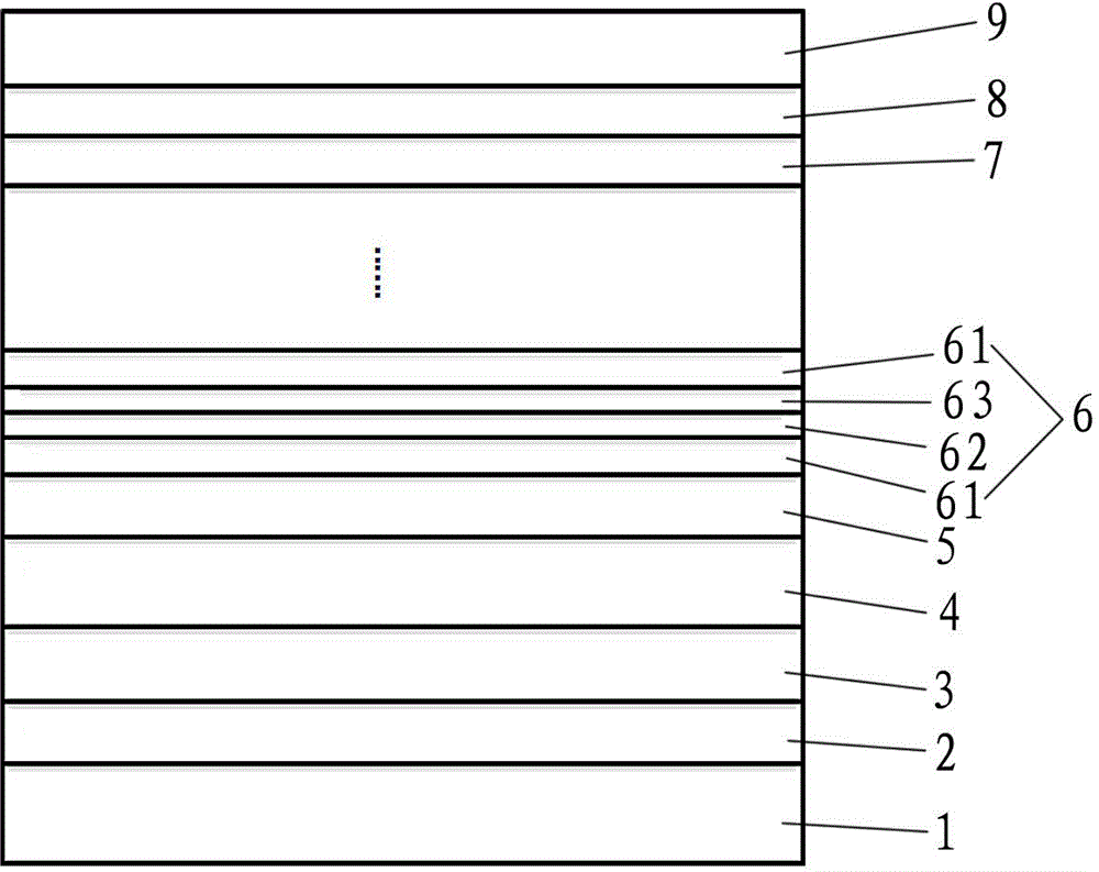
[0056] like figure 1 As shown, the present invention discloses an LED epitaxial structure with a high-quality InGaN / GaN active layer, on which a buffer layer 2, an unintentionally doped layer 3, an N-type doped layer 4, and a stress balance layer are sequentially grown on a substrate 1. Layer 5, In x Ga 1-x N / GaN active layer 6, hole injection layer 7, electron blocking layer 8 and P-type doped layer 9; In x Ga 1-x The N / GaN active layer 6 is composed of multiple sets of GaN quantum barrier layers 61 and In x Ga 1-x N quantum well layer 62 is formed. In each set of GaN quantum barrier layers 61 and In x Ga 1-x A GaN protective layer 63 is grown between the N quantum well layers 62 .

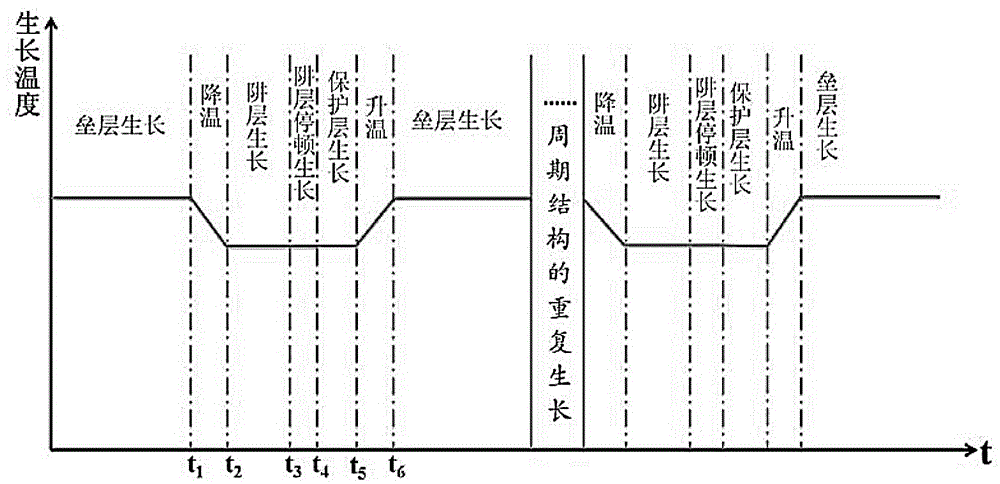
[0057] The present invention also discloses a method for growing an LED epitaxial structure with a high-quality InGaN / GaN active layer. On a substrate 1, a buffer layer 2, an unintentionally doped layer 3, an N-type doped layer 4, a stressed Balance layer 5, In x Ga 1-x N / GaN active la...

Embodiment 2

[0076] The difference from Embodiment 1 is that: Figure 5 As shown, a GaN / InGaN superlattice layer 10 is grown between the hole injection layer 7 and the electron blocking layer 8, through the growth of the superlattice layer 10, the crystal quality and hole concentration can be further improved.

[0077] In this embodiment, a method for growing an LED epitaxial structure with a high-quality InGaN / GaN active layer, a buffer layer 2, an unintentionally doped layer 3, an N-type doped layer 4, and a stress balance layer are sequentially grown on a substrate 1. Layer 5, In x Ga 1-x N / GaN active layer 6, hole injection layer 7, electron blocking layer 8 and P-type doped layer 9, GaN / InGaN superlattice layer 10 is grown between hole injection layer 7 and electron blocking layer 8; wherein, In x Ga 1-x The growth of N / GaN active layer 6 comprises the following steps:

[0078] Using MOCVD equipment to epitaxially grow high-brightness green light-emitting diodes, a 2-inch c-plane...


PUM

PropertyMeasurementUnit
Thicknessaaaaaaaaaa

Abstract

The invention discloses a method for growing an LED epitaxial structure with a high-quality InGaN/GaN active layer. The InGaN/GaN active layer is grown by use of the steps of introducing a Ga source and NH3 to grow a GaN barrier layer of 8-5nm in the atmosphere of H2 serving as a main carrier gas, switching the main carrier gas to N2 and introducing the Ga source, an In source and the NH3 to grow an InxGa1-xN trap layer of 2-5nm, shutting down the Ga source and the In source while keeping normal introduction of the NH3 to stop the growth of the InxGa1-xN, turning on the Ga source to grow a GaN protective layer of 1-5nm, switching the main carrier gas to the H2 and introducing the Ga source and the NH3 to grow the GaN barrier layer of 8-5nm, and finally, repeating the second to fifth growth steps for 1-20 cycles. The method for growing the LED epitaxial structure with the high-quality InGaN/GaN active layer is capable of obtaining the high-quality InGaN/GaN active layer and improving the LED luminous efficiency.

Description

technical field [0001] The invention relates to the field of LED technology, in particular to a method for growing an LED epitaxial structure with a high-quality InGaN / GaN active layer. Background technique [0002] GaN-based blue-green light-emitting diodes have the advantages of small size, long life, low power consumption, high brightness, and easy integration. In the prior art, the growth of GaN-based blue-green LED materials is mainly carried out by metal-organic chemical vapor deposition (MOCVD) epitaxial growth. Due to the high price of GaN substrates, in order to save costs, GaN-based blue-green LEDs are usually heterogeneously epitaxy on sapphire, silicon carbide and other substrates. Due to the problems of lattice mismatch and thermal mismatch in heteroepitaxy, it is difficult to obtain GaN-based blue-green LED epitaxial wafers with high crystal quality. [0003] In the prior art, blue and green light LEDs use the alloy InGaN material of GaN and InN as the light-...

Claims


Application Information

Patent Timeline
IPC IPC(8): H01L33/30H01L33/00
CPCH01L33/0075H01L33/32H01L2933/0008
Inventor 卓祥景陈凯轩林志伟蔡建九张永姜伟林志园尧刚
Owner XIAMEN CHANGELIGHT CO LTD
Why Eureka
Try Eureka