Tunneling field-effect transistor and manufacturing method thereof

A technology of tunneling field effect and manufacturing method, applied in semiconductor/solid-state device manufacturing, semiconductor devices, electrical components, etc., can solve the problems of leakage current destroying sub-threshold swing, impurity diffusion distribution, difficult device turn-off, etc., to improve Sub-threshold characteristics, improving on-current, and realizing the effect of device turn-off

Active Publication Date: 2015-02-11
INST OF MICROELECTRONICS CHINESE ACAD OF SCI
View PDF7 Cites 3 Cited by
  • Summary
  • Abstract
  • Description
  • Claims
  • Application Information

AI Technical Summary

Problems solved by technology

However, in order to reduce the sub-threshold swing and increase the conduction current, the tunneling junction needs to be as narrow as possible. However, the tunneling field-effect transistor with the existing structure will always cause the diffusion distribution of impurities during the implantation and heat treatment processes, and it is difficult to achieve a narrow junction. tunneling knot
[0005] In addition, in conventional tunneling field effect transistors, the source and drain regions are highly doped, and the doping will inevitably introduce defects, and the leakage current associated with these defects will destroy the reduction of the subthreshold swing.
Moreover, conventional tunneling field effect transistors have bipolar characteristics that can be turned on at both positive and negative gate voltages, making it difficult to completely turn off the device

Method used


Image

  • Tunneling field-effect transistor and manufacturing method thereof
  • Tunneling field-effect transistor and manufacturing method thereof
  • Tunneling field-effect transistor and manufacturing method thereof

Examples


Embodiment Construction

[0050] Embodiments of the present invention are described in detail below, examples of which are shown in the drawings, wherein the same or similar reference numerals designate the same or similar elements or elements having the same or similar functions throughout. The embodiments described below by referring to the figures are exemplary only for explaining the present invention and should not be construed as limiting the present invention.

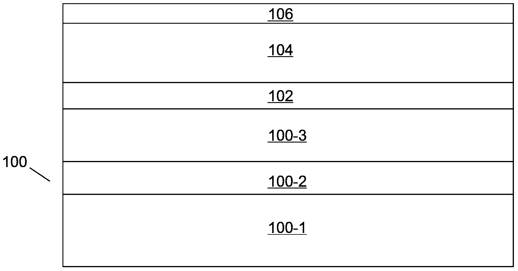
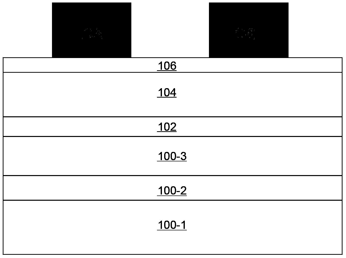
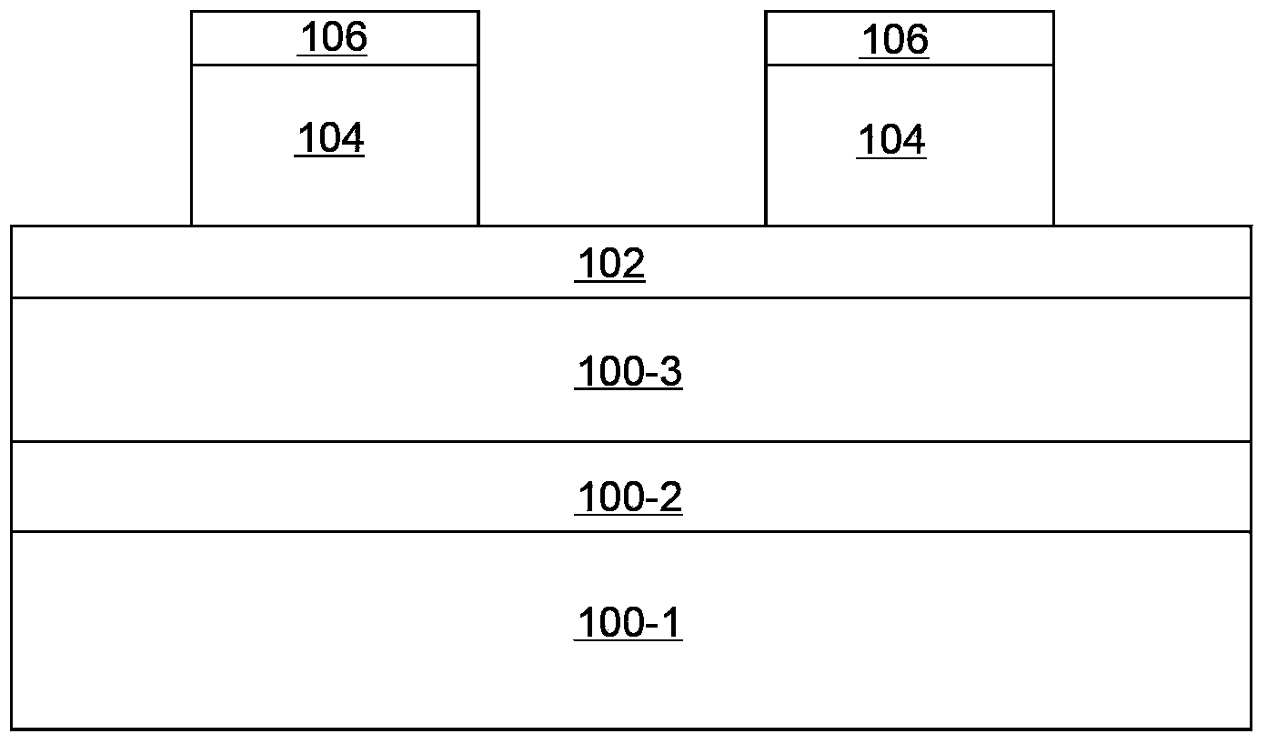
[0051] The present invention aims at proposing a new tunneling field effect transistor structure to overcome the difficulty in realizing a narrow tunneling junction in the existing tunneling field effect transistor structure, refer to Figure 40-42 ( Figure 40 for top view, Figure 41 , 42 respectively Figure 40 As shown in the LL', AA' direction view), the tunneling field effect transistor includes:

[0052] The substrate 100-1, 100-2 has a fin 140 on the substrate, and the fin 140 has an opposite first side, a second side, and an...


PUM


Abstract

The invention provides a tunneling field-effect transistor. The tunneling field-effect transistor includes a substrate, a first gate dielectric layer and a second gate dielectric layer, a first gate and a second gate as well as a first doped region and a second doped region; the substrate is provided with a fin; the fin is provided with a first side surface and a second side surface which are opposite to each other as well as a third side surface and a fourth side surface which are opposite to each other; the first gate dielectric layer and the second gate dielectric layer are formed on the first side surface and the second side surface respectively; the first gate and the second gate are formed on the substrate and are connected with the first gate dielectric layer and the second gate dielectric layer respectively; the first doped region and the second doped region are formed on the substrate and are connected with the third side surface and the fourth side surface respectively; and the first doped region and the second doped region have different doping types. According to the tunneling field-effect transistor of the invention, the width of a tunneling junction is controlled through the width of a fin channel region, and a larger and more effective tunneling area can be provided, and thus, conduction current can be increased; tunneling occurs in a semiconductor layer, namely in a channel, and a tunneling layer is un-doped or lowly-doped, and therefore, leakage current can be reduced, and the sub threshold characteristics of the device can be improved; and double-gate control is adopted, so that bipolar conduction characteristics can be better controlled, and the on-off of the device can be realized.

Description

technical field [0001] The invention relates to the field of semiconductor devices, in particular to a tunneling field effect transistor and a manufacturing method thereof. Background technique [0002] With the continuous shrinking of the device size, the number of devices per unit area of ​​the chip is increasing, and how to reduce power consumption has become an increasingly prominent problem. [0003] The structure of a conventional tunneling field-effect transistor (Normal-TFET) mainly includes a substrate (channel), a gate dielectric layer, a gate, and source / drain regions on both sides of the gate. It is mainly based on the quantum tunneling effect, with P-type tunneling field effect transistor as an example, when a negative voltage is applied to the gate, the potential of the channel region rises, quantum tunneling occurs from the source region to the channel region, and the electrons and holes generated by the tunneling pass from the source region to the drain regio...

Claims


Application Information

Patent Timeline
Patent Type & Authority Applications(China)
IPC IPC(8): H01L29/78H01L29/08H01L21/336
CPCH01L29/0684H01L29/0847H01L29/66795H01L29/7855H01L29/7856
Inventor 朱正勇朱慧珑许淼
Owner INST OF MICROELECTRONICS CHINESE ACAD OF SCI
Why Eureka
Try Eureka