Flip-chip bonding electrode structure of surface-type semiconductor laser device

A laser device and electrode structure technology, which is applied in the direction of semiconductor lasers, semiconductor devices, laser components, etc., can solve the problems of increasing the distance between P-type electrodes and N-type electrodes, and the height difference between P-type electrodes and N-type electrodes. Effects of increased distance, prevention of short-circuit conditions, and simple packaging process

Inactive Publication Date: 2015-02-25
BEIJING UNIV OF TECH
View PDF8 Cites 5 Cited by
  • Summary
  • Abstract
  • Description
  • Claims
  • Application Information

AI Technical Summary

Problems solved by technology

[0004] In order to solve the above-mentioned technical problems, the present invention provides a surface-type semiconductor laser device flip-chip welding electrode structure, which solves the

Method used


Image

  • Flip-chip bonding electrode structure of surface-type semiconductor laser device
  • Flip-chip bonding electrode structure of surface-type semiconductor laser device

Examples


Example Embodiment

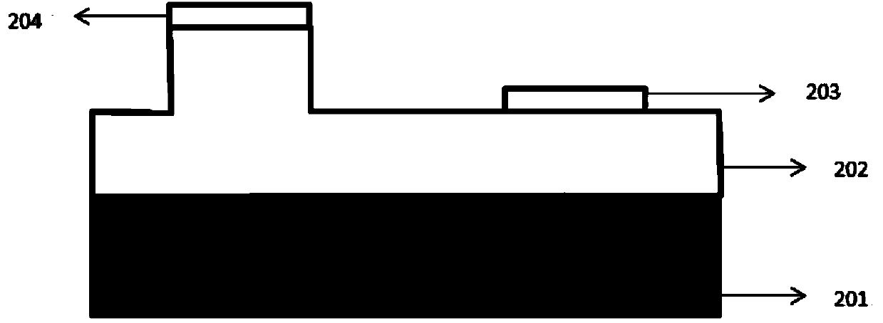
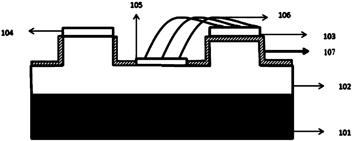
[0024] Such as figure 1 As shown, the surface type semiconductor laser device flip-chip electrode structure of the present invention includes: a sapphire substrate (101), an epitaxial growth layer (102), an N'-type electrode (103), a P-type electrode (104), and an N-type electrode (105), gold wire (106) and insulating layer (107).

[0025] The sapphire substrate (101) used as a laser medium is a substrate for growing other structures, and the main component is alumina (Al 2 O 3 ); And the sapphire substrate (101) is a trigonal crystal system, with a refractive index of 1.76 to 1.77, which is a heterogeneous body, without cleavage, and is a development of cracks.

[0026] The epitaxial growth layer (102) is deposited and grown layer by layer on the sapphire substrate by a metal organic compound chemical vapor deposition method.

[0027] The N-type electrode (105) and P-type electrode (104) are used to etch the epitaxial growth layer by photolithography, and then use evaporation or spu...


PUM


Abstract

The invention provides a flip-chip bonding electrode structure of a surface-type semiconductor laser device and belongs to the field of laser technology application. The flip-chip bonding electrode structure comprises a sapphire substrate, an epitaxial growth layer, an insulation layer, a P-type electrode, an N-type electrode, an N'-type electrode and a gold wire, wherein the N'-type electrode and the P-type electrode are equal in height and positioned on two sides of the N-type electrode respectively, and two ends of the gold wire are bonded on the N-type electrode and the N'-type electrode respectively. The flip-chip bonding electrode structure of the surface-type semiconductor laser device has the advantages that a traditional structure of the surface-type semiconductor laser device is changed, the height of the N-type electrode is increased to be as same as that of the P-type electrode through the gold wire, and accordingly, the problem of height difference between the P-type electrode and the N-type electrode of the sapphire laser device can be solved; in the same way, spacing between the P-type electrode and the N-type electrode can be increased properly, and bonding consumables of the P-type electrode and the N-type electrode can be isolated during bonding, so that short circuit possibly happening during bonding is prevented effectively.

Description

technical field [0001] The invention belongs to the technical field of semiconductor laser preparation and packaging, and in particular relates to a surface-type semiconductor laser device flip-chip welding electrode structure. Background technique [0002] With the maturity of semiconductor laser technology and the continuous expansion of application fields, the application range of semiconductor laser devices has covered many fields of optoelectronics, and has become the core technology of today's optoelectronic practical devices. Due to the advantages of small size, light weight and long life, semiconductor laser devices are widely used in military, industrial and civilian fields. Sapphire is known as one of the best laser media today, not only has good thermal conductivity and mechanical properties, high saturation flux, more importantly, its wavelength tuning range wider than 500nm is unmatched by any existing laser media of. Semiconductor laser devices based on sapph...

Claims


Application Information

Patent Timeline
IPC IPC(8): H01L33/62H01S5/022
CPCH01L33/62H01S5/0231H01S5/0234
Inventor 尧舜雷宇鑫王智勇邱运涛贾冠男高祥宇吕朝蕙
Owner BEIJING UNIV OF TECH
Why Eureka
Try Eureka