
Eureka
For R&D, Eureka makes reading and utilizing patents & technical documents easy.
Eureka AIR
Designed for self-driven R&D workflows. Generate viable solutions, solve complex R&D challenges, empower your innovation with AI.

Eureka Materials
Designed for material experts only. Revolutionize your material R&D, from search, analyze, to developing new materials.

TechResearch
Generate reliable direction feasibility study reports for your R&D in just a few steps.

TechSeek
Discover and master advanced knowledge NOW. Basics, ideas, possibilities, all at once.

TechMind
As an expert in R&D Theories, TechMind can generates customized viable solutions instantly.

TechRisk
Analyze your overall solution with one click, know your potential R&D risks in advance.

TechMonitor
Get weekly tech updates, stay abreast of the latest tech innovations and key insights.
Radiological volt isotope battery and preparation method thereof
A technology of isotope battery and radiant volt, which is applied in the field of micro-energy, to achieve the effects of reducing carrier transport recombination loss, convenient loading, and reducing energy loss
- Summary
- Abstract
- Description
- Claims
- Application Information
AI Technical Summary
Problems solved by technology
Method used
Image

Examples
Embodiment 1
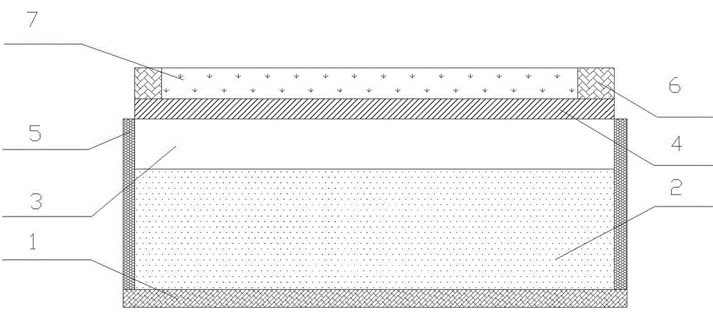
[0027] Such as figure 1 Among them, the resistivity is chosen to be 0.002Ω·cm -1 N + Type silicon substrate layer 2 is used as the substrate, and N-type doped epitaxial growth is carried out by LPCVD to form a doping concentration of 1×10 16 cm -3 , an epitaxial N-type silicon layer 3 with a thickness of 6 μm; an Au Schottky barrier metal layer 4 is patterned and evaporated on the epitaxial layer after surface treatment on the epitaxial silicon wafer, with a thickness of 30 nm; patterned evaporation is deposited on the metal surface of the barrier layer Au upper electrode 6 with a thickness of 1 micron; a Ti layer with a thickness of 0.7 micron is patterned and evaporated on the metal surface of the barrier layer; a 1 micron thick Au, Ag or Al lower electrode metal layer is evaporated after surface treatment on the back of the base layer 1; Scribing; Ti layer chemisorption tritium loading radioactive source at high temperature.
Embodiment 2
[0029] Such as figure 1 Among them, the lower electrode metal layer 1 is Ti / Ni / Au with a thickness of 1 micron, N + Type silicon substrate layer 2 resistivity is 0.002Ω·cm -1 , the doping concentration of the epitaxial N-type silicon layer 3 is 8×10 15 cm -3 , the thickness is 20 μm, the Schottky barrier metal layer 4 is Au, the thickness is 30nm; the insulating passivation layer 5 is silicon dioxide, the thickness is 100nm, the upper electrode metal 6 is Au with a thickness of 1 μm, and the radioactive isotope layer 7 for electroplating 63 Ni.
Embodiment 3
[0031] Such as figure 1 , the lower electrode metal layer 1 is 1 micron thick Au, N + Type silicon substrate layer 2 resistivity is 0.002Ω·cm -1 , the doping concentration of the epitaxial N-type silicon layer 3 is 5×10 15 cm -3 , the thickness is 30 μm, the Schottky barrier metal layer 4 is a 50nm sputtered Pt metal layer, the insulating passivation layer 5 is silicon dioxide, the thickness is 100nm, the upper electrode metal 6 is Au with a thickness of 1 μm, and a radioactive isotope layer is loaded 7 for electroplating 147 Pm.
PUM
| Property | Measurement | Unit |
|---|---|---|
| thickness | aaaaa | aaaaa |
| thickness | aaaaa | aaaaa |
| thickness | aaaaa | aaaaa |
Abstract
Description
Claims
Application Information
 - R&D Engineer
- R&D Manager
- IP Professional
- Industry Leading Data Capabilities
- Powerful AI technology
- Patent DNA Extraction
Browse by: Latest US Patents, China's latest patents, Technical Efficacy Thesaurus, Application Domain, Technology Topic, Popular Technical Reports.
© 2024 PatSnap. All rights reserved.Legal|Privacy policy|Modern Slavery Act Transparency Statement|Sitemap|About US| Contact US: help@patsnap.com