Unlock instant, AI-driven research and patent intelligence for your innovation.

Three-dimensional carbon nano wire transistor structure and preparation method thereof

A carbon nanowire and transistor technology, applied in the field of three-dimensional carbon nanowire transistor structure and its preparation, can solve the problems of inability to manufacture three-dimensional transistors, limit the area utilization rate of silicon wafers, etc., so as to improve the area utilization rate, reduce occupation, and ensure The effect of practicality

Inactive Publication Date: 2015-03-04
SHANGHAI INTEGRATED CIRCUIT RES & DEV CENT +1
View PDF4 Cites 6 Cited by
  • Summary
  • Abstract
  • Description
  • Claims
  • Application Information

AI Technical Summary

Problems solved by technology

The manufacture of traditional silicon transistor MOSFETs limits the further improvement of transistor density, limits the utilization rate of silicon chip area, and cannot make three-dimensional stacked interconnected transistors

Method used


Image

  • Three-dimensional carbon nano wire transistor structure and preparation method thereof
  • Three-dimensional carbon nano wire transistor structure and preparation method thereof
  • Three-dimensional carbon nano wire transistor structure and preparation method thereof

Examples


preparation example Construction

[0032] The invention provides a three-dimensional carbon nanowire transistor structure and a preparation method thereof, which can manufacture smaller transistors to increase transistor density, increase the width-to-length ratio of transistors, and improve the area utilization rate of silicon wafers.

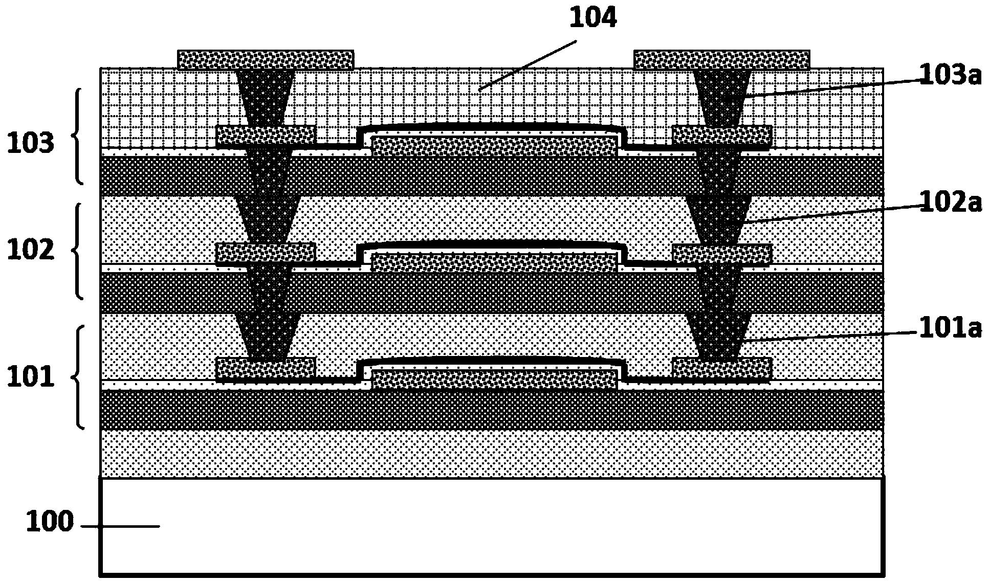
[0033] Such as figure 1Shown is the cross-sectional structure of the three-dimensional carbon nanowire transistor structure provided by the present invention. Although the illustration only shows the superposition of three device layers, in actual operation, more device layers can be added according to product needs, and the device width-to-length ratio can be increased by connecting more carbon nanowire transistors in parallel. In the figure, 101, 102 and 103 are the device layers arranged with the same carbon nanowire transistors, through the through holes 101a, 102a, the interconnection between the corresponding poles of the carbon nanowire transistors in the upper and lower...

Embodiment

[0035] Hereinafter, the preparation method of the three-dimensional carbon nanowire transistor structure provided by the present invention will be described in detail.

[0036] In order to avoid tedious repetition, this embodiment only selects a three-dimensional carbon nanowire transistor structure with two device layers for detailed introduction.

[0037] Such as Figure 2a As shown, an insulating dielectric layer SiO2 is grown on a silicon substrate 100 by a thermal oxidation process, with a thickness of 30-50 nanometers. Since the carbon nanowire transistor provided by the present invention is different from traditional transistors, it is not necessary to connect the source, drain, gate, and three electrodes to the substrate, so the silicon substrate 100 is the supporting substrate here. Because in actual application, the structure of the present invention may share the substrate with other devices, and since the present invention uses a back gate design, the deposition o...


PUM

PropertyMeasurementUnit
Thicknessaaaaaaaaaa
Thicknessaaaaaaaaaa
Thicknessaaaaaaaaaa

Abstract

The invention relates to a three-dimensional carbon nano wire transistor structure comprising a support substrate and a multi-layer device layer. The multi-layer device layer is arranged on the support substrate and contains polyimide films and a carbon nano wire transistors; the layers are separated from each other and are stacked; and transistors of all layers are connected in parallel. In addition, the invention also provides a preparation method of the three-dimensional carbon nano wire transistor structure. Carbon nano wire transistors are established on a polyimide film deposited on a silicone substrate to form a device layer; a dielectric isolation unit is deposited; an interconnection access of the grid electrodes and source / drain electrodes of the transistors at the upper layer and the lower layer is established by a through hole; a polyimide film is repeatedly deposited on the device layer to prepare an upper layer device layer; and the layers are repeatedly prepared and stacked, thereby realizing a three-dimensional interconnected transistor structure. According to the invention, a plurality of same types of carbon nano wire transistors in parallel connection are prepared at the same silicon substrate area, thereby improving the transistor density, increasing the transistor breadth length ratio, and enhancing the silicon wafer area utilization rate. Moreover, the preparation process is compatible with the traditional CMOS process completely.

Description

technical field [0001] The invention relates to the technical field of semiconductors, in particular to a three-dimensional carbon nanowire transistor structure and a preparation method thereof. Background technique [0002] The traditional transistor MOSFET is fabricated on a single crystal silicon substrate material. Driven by the continuous pursuit of Moore's Law, the channel length of traditional transistor MOSFETs has been continuously reduced, and the device size has been reduced. This shrinkage increases transistor density, improves chip integration, and other fixed factors and switching speeds, while reducing power consumption and continuously improving chip performance. In the future, as the technical requirements continue to improve, and silicon chips cannot be made smaller, new chip manufacturing materials must be found, and carbon nanotransistors will be a good choice. [0003] The so-called carbon nanotubes are tiny cylinders formed by carbon atoms. They have ...

Claims


Application Information

Patent Timeline
IPC IPC(8): H01L29/775H01L21/335B82Y10/00
CPCB82Y10/00H10K85/221H10K10/00H10K10/46
Inventor 任铮郭奥胡少坚周伟
Owner SHANGHAI INTEGRATED CIRCUIT RES & DEV CENT