An induction reflow soldering device and a circuit board component welding method using the device

A technology for reflow soldering and circuit boards, applied in welding equipment, manufacturing tools, metal processing, etc., can solve problems such as unsuitable use of electrostatic sensitive devices, tombstone of small-volume SMT devices, poor thermal stress tolerance, etc. The effect of uneven heating of points, elimination of warping or delamination, and reduction of strength requirements

Active Publication Date: 2016-06-01
张楠
View PDF7 Cites 0 Cited by
  • Summary
  • Abstract
  • Description
  • Claims
  • Application Information

AI Technical Summary

Problems solved by technology

[0002]Existing induction welding tools generally place the soldering iron tip in the solenoid coil, and use the high-frequency current in the coil to form a high-frequency alternating current in the soldering iron tip. The magnetic field, and then the eddy current loss generated in the soldering iron head by this magnetic field makes the soldering iron head heat up for soldering, which has the advantage of fast heating up, but it has the same defects as ordinary constant temperature soldering irons, and some SMD components cannot be soldered, especially with Surface array package is the representative chip component, because many of the soldering pads of these widely used chip components are located at the bottom of the integrated block, and the tip of the soldering iron cannot enter the soldering at all.
[0003]In the electronic manufacturing industry, in order to solve this kind of problem, reflow soldering technology is widely used, and in the existing reflow soldering equipment using air or nitrogen as the medium , not only the printed board (PCB) and all the components on the printed board have to bear the high temperature circulating gas enough to melt the solder, it is easy to cause the failure of the components with poor thermal stress tolerance, and it is easy to cause the deformation of the printed board and Delamination, especially with the widespread use of lead-free solders today, is aggravated by the fact that the melting point of lead-free solder pastes is generally higher than that of tin-lead solder pastes
At the same time, due to the inherent shortcomings of some equipment: for example, airflow causes small-volume SMD devices to tombstone and skew; uneven temperature caused by various reasons leads to uneven heating of solder joints, welding quality problems such as virtual soldering, which directly affect the yield.
Therefore, the actual heating effect of Documents 1 and 2 is limited by the size of the target heating object, and it can only be heated for larger solder balls or modules, and reflow soldering for integrated circuit devices with only small-volume copper pads The heating is extremely limited
2. In Document 1 and Document 2, the existing induction heating equipment is used to generate alternating electromagnetic fields, which require a relatively strong alternating magnetic field. The stronger the generated alternating electromagnetic field, the greater the apparent power required, and Electromagnetic radiation is also very serious
3. In Document 1 and Document 2, it is suitable for the local heating of a device on the entire circuit board, but the difference in temperature rise between the solder joints of the devices after the distribution of multiple different devices on the circuit board cannot be uniformly controlled. When the entire circuit board is heated in the same high-frequency alternating magnetic field, it is easy to cause overheating of the solder joints of the components that heat up quickly, and the solder joints of the components that heat up slowly have not yet melted.
4. Documents 1 and 2 both use infrared sensors to sample the temperature of the target device in reflow soldering. The infrared sensor can only sample the temperature on the surface of the device, but the temperature of the solder point below the surface of the device cannot be directly measured. It is obvious that for SMD components with different thicknesses, heat transfer coefficients, and packages on a circuit, the difference between the surface temperature of the device and the temperature of the solder joint below the device is also different, and it is impossible to reasonably control the soldering temperature of the entire board. Temperature is one of the most core process parameters in whole board welding, and generally needs to be directly preset and monitored in time
[0005] The induction reflow soldering equipment also mentioned in the information on the Internet uses a transformer in the heating head, and uses the principle of inductive eddy current to weld the weldment. This welding method has no mechanical Contact, fast heating; the disadvantage is that it is sensitive to position, difficult to control temperature, and there is a risk of overheating, and electrostatic sensitive devices should not be used

Method used


Image

  • An induction reflow soldering device and a circuit board component welding method using the device
  • An induction reflow soldering device and a circuit board component welding method using the device
  • An induction reflow soldering device and a circuit board component welding method using the device

Examples


Embodiment Construction

[0038] In order to clearly illustrate the technical features of the solution, the solution will be described below through a specific implementation mode combined with the accompanying drawings.

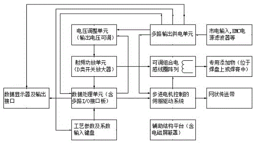
[0039] The invention provides a method for implementing induction reflow soldering, including a professional equipment induction reflow soldering system suitable for industrial applications and a miniaturized induction reflow soldering system that is convenient for personal use. All the SMD components on the board are induction welded continuously, quickly and efficiently at the same time, and in the case of expanding the size of the adjustable coil array, simultaneous welding of multiple printed boards is realized. The miniaturized system is used to complete the induction welding of a single SMT component on a single printed board. The block diagram of the induction welding system for professional equipment is shown in figure 1 As shown, the miniaturized system simply omits the fi...


PUM

PropertyMeasurementUnit
lengthaaaaaaaaaa
Curie pointaaaaaaaaaa

Abstract

The invention provides a technical scheme of an induction reflow soldering device and a welding method for circuit board components using the device. The scheme includes a main machine, an inductance coil array and a transmission belt; The magnetic cylinders are arranged in the same direction; the solenoid coil is wound on the magnetic rod; the inductance coil array is arranged above the transmission belt; this scheme allows the adjustable combined inductance coil array to be used not only as an energy output device, but also as a sampling device for the temperature of the solder point. Utilizing the 5 physical and chemical properties of the additives, under the control of the host, the induction reflow soldering with features such as direct monitoring of solder joint temperature, automatic solder joint temperature uniformity, dynamic optimization of the welding process, and high efficiency and energy saving is realized.

Description

technical field [0001] The invention relates to the field of electronic manufacturing and application, in particular to an induction reflow soldering device and a circuit board component welding method using the device. Background technique [0002] The existing induction welding tools generally place the soldering iron tip in the solenoid coil, and use the high-frequency current in the coil to form a high-frequency alternating magnetic field in the soldering iron tip, and then use the eddy current loss generated in the soldering iron tip by this magnetic field to make the The soldering iron head heats up for soldering, which has the advantage of fast heating, but it has the same defects as ordinary constant temperature soldering irons, and some SMD components cannot be soldered, especially SMD components represented by area array packages, because these widely used Many pads that need to be soldered for SMD components are located at the bottom of the integrated block, and t...

Claims


Application Information

Patent Timeline
Patent Type & Authority Patents(China)
IPC IPC(8): B23K1/002B23K3/00
CPCB23K1/0016B23K1/002B23K1/203B23K3/00
Inventor 张楠
Owner 张楠
Why Eureka
Try Eureka