Outline dicing and sheet picking method for ultrathin quartz substrate thin film circuit

A thin-film circuit and circuit graphics technology, which is applied to circuits, electrical components, grinding machines, etc., can solve problems such as direct and effective pick-up of difficult workpieces, scratches on the surface of the circuit, and collapse of the shape of the thin-film circuit, so as to achieve a good circuit appearance , easy to wrap, low cost effect

Active Publication Date: 2015-03-11
CHINA ELECTRONIS TECH INSTR CO LTD
View PDF4 Cites 0 Cited by
  • Summary
  • Abstract
  • Description
  • Claims
  • Application Information

AI Technical Summary

Problems solved by technology

However, the automatic sheet unloading machine is currently only suitable for picking up the workpiece from the adhesive film through the steps of adhesive film expansion, film removal and vacuum adsorption after scribing, and is not suitable for the workpiece using an adhesive with high bond strength ( Such as glue, paraffin, etc.) bonded to the hard substrate and cut
Because the workpiece is directly bonded to the hard substrate with a high-strength adhesive, after cutting, it needs to be soaked in a special solvent to remove the adhesive. After cleaning, there is a small amount of residual solvent at the bottom of the container, which will separate the workpiece from the substrate. The air at the bottom

Method used


Image

  • Outline dicing and sheet picking method for ultrathin quartz substrate thin film circuit
  • Outline dicing and sheet picking method for ultrathin quartz substrate thin film circuit
  • Outline dicing and sheet picking method for ultrathin quartz substrate thin film circuit

Examples


Embodiment 1

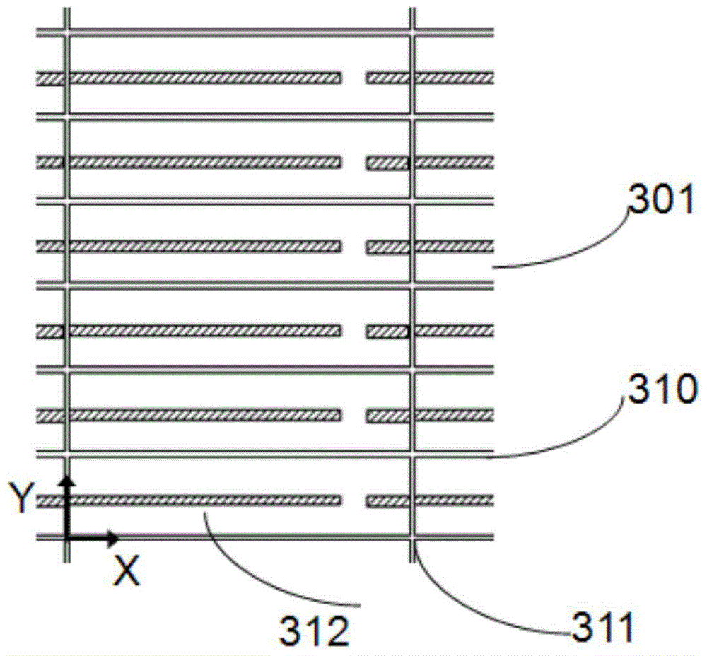
[0049] Scribe and cut a rectangular thin film circuit in the form of a 3×22 array on a square ultra-thin quartz substrate with a thickness of 50 μm and a plane size of 20mm×20mm. The slits in the X direction and the Y direction are both 80 μm in size. The surface and the back are metal-free film surfaces. The plane size of the film circuit pattern is 4.8mm×0.3mm, and the aspect ratio is 16:1.

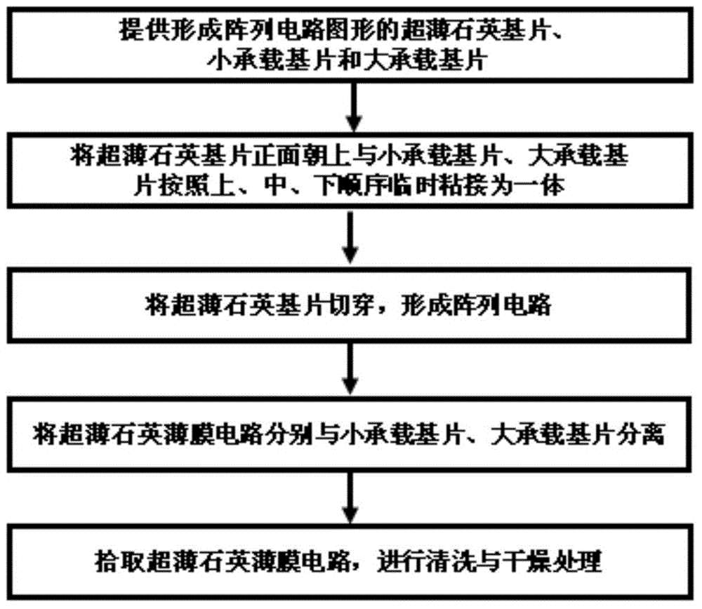
[0050] Step 1, providing an ultra-thin quartz substrate, a small carrying substrate and a large carrying substrate for forming an array circuit pattern.

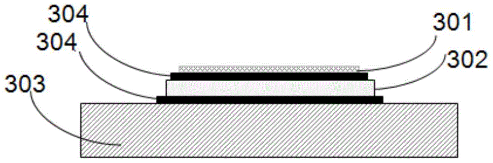
[0051] First, provide a 50 μm thick square ultra-thin quartz substrate 301 with a plane size of 20mm×20mm, the front side is a surface for forming an array circuit pattern, and the back side is a metal-free film surface; then prepare a 0.5mm thick, plane size 25.4mm×25.4 mm square quartz glass is used as the small carrier substrate 302; and a square quartz glass with a thickness of 1.5 mm and a plane size of 76.2 mm×76.2 mm is prepare...

Embodiment 2

[0061]Scribe a 2×21 thin-film circuit in an array form on a square ultra-thin quartz substrate with a thickness of 30 μm and a plane size of 20mm×20mm. The slits in the X direction and the Y direction are both 50 μm in size. The back side is a full-board thin-film metallization ground plane, the plane size of the thin-film circuit pattern is 7.8mm×0.2mm, and the aspect ratio is 39:1.

[0062] Step 1, providing an ultra-thin quartz substrate, a small carrying substrate and a large carrying substrate for forming an array circuit pattern.

[0063] First, provide a 30 μm thick square ultra-thin quartz substrate 301 with a plane size of 20mm×20mm. A square quartz glass of mm×25.4 mm is used as the small carrier substrate 302 ; and a square quartz glass with a thickness of 1 mm and a planar size of 76.2 mm×76.2 mm is prepared as the large carrier substrate 303 .

[0064] Step 2, bonding the ultra-thin quartz substrate with the front side up to the small carrier substrate and the la...

Embodiment 3

[0073] Scribe and cut a double-sided film circuit in the form of a 5×20 array on a square ultra-thin quartz substrate with a thickness of 50 μm and a plane size of 20 mm×20 mm. , the back is an array circuit graphic surface that is symmetrical to the front circuit graphic, the plane size of the thin film circuit graphic is 2.4mm×0.3mm, and the aspect ratio is 8:1.

[0074] Step 1, providing an ultra-thin quartz substrate, a small carrying substrate and a large carrying substrate for forming an array circuit pattern.

[0075] First provide a square ultra-thin quartz substrate 301 with a thickness of 50 μm, with a plane size of 20mm×20mm, the front is a surface for forming an array circuit pattern, and the back is a surface for forming an array circuit pattern symmetrical to the front circuit pattern; then prepare a 0.5mm thick, A square quartz glass with a planar size of 25.4mm×25.4mm is used as the small carrier substrate 302;

[0076] Step 2, bonding the ultra-thin quartz su...


PUM

PropertyMeasurementUnit
Thicknessaaaaaaaaaa
Areaaaaaaaaaaa
Widthaaaaaaaaaa

Abstract

The invention discloses an outline dicing and sheet picking method for an ultrathin quartz substrate thin film circuit. The method comprises the following steps: providing an ultrathin quartz substrate, a small bearing substrate and a large bearing substrate forming an array circuit pattern; temporarily bonding the ultrathin quartz substrate (right side up) integrally with the small bearing substrate and the large bearing substrate from top to middle to bottom; cutting through the ultrathin quartz substrate to form an array circuit; separating the ultrathin quartz thin film circuit from the small bearing substrate and the large bearing substrate respectively; and picking up the ultrathin quartz thin film circuit, and performing cleaning and drying treatment. The method is easy to operate. Moreover, the circuit is complete in appearance and good in shape, and the yield is increased greatly.

Description

technical field [0001] The invention belongs to the technical field of millimeter-wave and sub-millimeter-wave integrated circuit manufacturing, and in particular relates to a shape cutting and picking method for thin-film circuits of ultra-thin quartz substrates. Background technique [0002] Quartz substrates are commonly used as circuit substrates for components in the terahertz frequency band. The material is high-purity isotropic fused silica. The reason is that the dielectric constant of quartz is relatively stable in the hundreds of GHz frequency band, and the loss is lower than that in the current microwave and millimeter wave frequency bands. The substrate material is also relatively stable in terms of thermal and mechanical properties. Quartz substrate thin film circuit patterns are usually prepared by large substrates and multi-units in the semiconductor integrated circuit process. The process includes: substrate cleaning, coating, photoetching, electroplating thi...

Claims


Application Information

Patent Timeline
IPC IPC(8): H01L21/78B24B27/06
CPCH01L21/707H01L21/78
Inventor 曹乾涛孙建华胡莹璐王斌邓建钦路波
Owner CHINA ELECTRONIS TECH INSTR CO LTD
Why Eureka
Try Eureka