

Epitaxial growth method for GaN-based LED epitaxial active area basic structure
A basic structure and epitaxial growth technology, which is applied in the field of epitaxial growth of the basic structure of the GaN-based LED epitaxial active region, can solve the problems of not being used by ordinary devices and high cost, and achieve the effect of smooth surface without defects and improved crystal quality
- Summary
- Abstract
- Description
- Claims
- Application Information
AI Technical Summary
Problems solved by technology
Method used
Image

Examples
Embodiment Construction
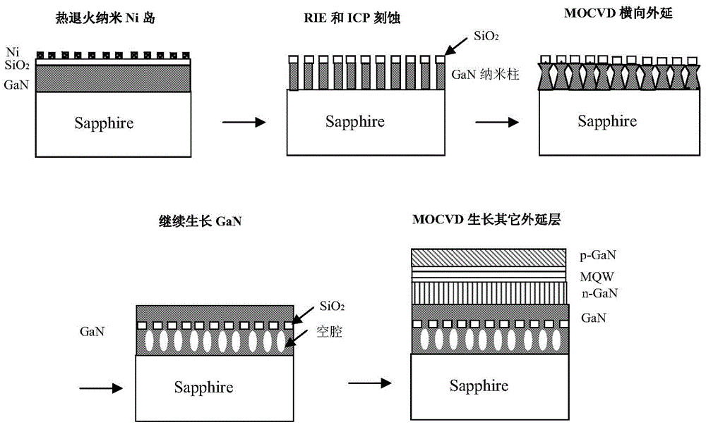
[0021] According to the principle of the present invention, as figure 2 As shown, the method for manufacturing high-brightness GaN-based LED epitaxial layer mainly includes the following steps:
[0022] 1. PECVD deposition of 200-300nm SiO on the 1.5-2.0μm thick GaN epitaxial layer 2 layer at a deposition temperature of 250 °C. Then in SiO 2 A layer of 8-15nm thick Ni film is vapor-deposited on the top, and Ni nano-islands are formed by rapid thermal annealing under a nitrogen atmosphere, the annealing temperature is 850°C, and the time is 1-3min.
[0023] 2. Using Ni nano-islands as a mask, use reactive ion etching (RIE) to etch SiO 2 layer, the etchant gas is CF 4 , the etching rate is controlled at 50-66nm / min, and the etching time is 3-6min. Continue to etch GaN using inductively coupled plasma etching (ICP) with an etching gas of 5 sccm of Cl 2 and 50 sccm of Ar, the etching rate is 45-58nm / min, and the time is 25-45min.
[0024] 3. HNO at 100°C 3 Soak in the sol...
PUM
| Property | Measurement | Unit |
|---|---|---|
| The average diameter | aaaaa | aaaaa |
| Average width | aaaaa | aaaaa |
| Average height | aaaaa | aaaaa |
Abstract
Description
Claims
Application Information