Method for preparing mask layer of III family compound substrate

A compound and mask layer technology, applied in semiconductor/solid-state device manufacturing, electrical components, circuits, etc., can solve problems such as chip quality reduction, chip value increase, GaN epitaxial layer surface damage, etc., and achieve a large etching depth Effect

Active Publication Date: 2015-03-18
BEIJING NAURA MICROELECTRONICS EQUIP CO LTD
View PDF5 Cites 9 Cited by
  • Summary
  • Abstract
  • Description
  • Claims
  • Application Information

AI Technical Summary

Problems solved by technology

[0019] During the mask deposition step, it is necessary to deposit SiO by vapor phase deposition 2 Or SiN mask, during this process, the plasma will etch the surface of the GaN epitaxial layer due to the self-bias generated on the substrate, resulting in damage to the surface of the GaN epitaxial layer, resulting in an increase in the VF (pre-stage voltage) value of the chip, and then reduce chip quality

Method used


Image

  • Method for preparing mask layer of III family compound substrate
  • Method for preparing mask layer of III family compound substrate
  • Method for preparing mask layer of III family compound substrate

Examples


Embodiment Construction

[0046] In order to enable those skilled in the art to better understand the technical solution of the present invention, the method for preparing the mask layer of the group III compound substrate provided by the present invention will be described in detail below with reference to the accompanying drawings.

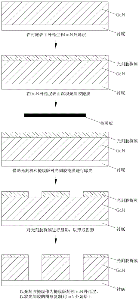
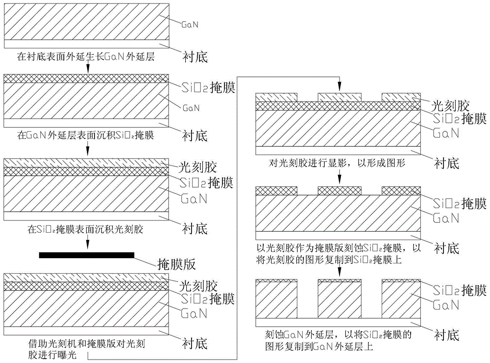
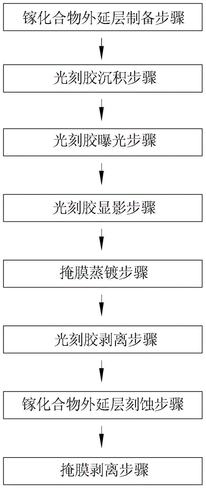
[0047] image 3 A flowchart of a method for preparing a mask layer of a group III compound substrate provided in an embodiment of the present invention. Figure 4 A schematic flowchart of a method for preparing a mask layer of a group III compound substrate provided in an embodiment of the present invention. Please also refer to image 3 and Figure 4 , the mask layer preparation method comprises the following steps:

[0048]The step of preparing the gallium compound epitaxial layer is to epitaxially grow the gallium compound epitaxial layer on the surface of the substrate. Wherein, the gallium compound epitaxial layer includes gallium nitride or gallium arsenide; th...


PUM


Abstract

The invention provides a method for preparing a mask layer of a III family compound substrate. The method comprises the following steps of depositing a photoresist, namely depositing the photoresist on the surface of an epitaxial layer of a gallium compound; exposing the photoresist; developing the photoresist, namely developing the exposed photoresist; evaporating the mask layer, namely evaporating at least one isolation layer on the surface of the photoresist and on the surface, uncovered by the photoresist, of the epitaxial layer of the gallium compound, and evaporating at least one metal layer on the surface of the isolation layer, wherein the isolation layer is made of a material capable of preventing a metal material of the metal layer from spreading to the epitaxial layer of the gallium compound, and the metal layer is made of a material capable of improving an etching selection ratio of the mask layer to the epitaxial layer of the gallium compound; peeling the photoresist, namely peeling the photoresist and the isolation layer and the metal layer on the photoresist. According to the method for preparing the mask layer of the III family compound substrate, the etching selection ratio of the mask layer to the epitaxial layer of the gallium compound is improved on the premise of not damaging the surface of the epitaxial layer of the gallium compound.

Description

technical field [0001] The invention relates to the technical field of semiconductor etching, in particular to a method for preparing a mask layer of a group III compound substrate. Background technique [0002] GaN (gallium nitride)-based light-emitting diodes are widely used in image display, signal indication, lighting and basic research because of their excellent characteristics such as long life, shock resistance, shock resistance and high efficiency and energy saving. At present, in order to improve the luminous efficiency of LEDs, more and more manufacturers have begun to adopt the new etching technology of GaN deep groove etching, that is, etching a concave hole with a depth of about 8 μm on the GaN epitaxial layer of the III-group compound substrate. groove. [0003] figure 1 It is a schematic flow chart of an existing GaN deep trench etching process. The process mainly includes the following steps: [0004] The GaN epitaxial layer preparation step is to epitaxi...

Claims


Application Information

Patent Timeline
Patent Type & Authority Applications(China)
IPC IPC(8): H01L21/033H01L33/20
CPCH01L21/0271
Inventor 张君
Owner BEIJING NAURA MICROELECTRONICS EQUIP CO LTD
Why Eureka
Try Eureka