High-transfer-characteristic low-stray-capacitance embedded grid insulation tunneling enhanced transistor

A low parasitic capacitance, high transfer technology, applied in the direction of circuits, electrical components, semiconductor devices, etc., can solve the problems of increasing production costs, no improvement, large gate to source, etc.

Inactive Publication Date: 2015-03-25
SHENYANG POLYTECHNIC UNIV
View PDF5 Cites 2 Cited by
  • Summary
  • Abstract
  • Description
  • Claims
  • Application Information

AI Technical Summary

Problems solved by technology

Although the degradation of this device performance can be alleviated by improving the structure of the gate electrode, when the device size is further reduced, the transfer characteristics of the device will deteriorate again
[0003] On the other hand, with the continuous reduction of device size, the distance between the drain electrode and the gate electrode, or the distance between the source electrode and the gate electrode is also continuously reduced, which makes the gate-source, source-gate of the device , Gate-to-drain and drain-gate parasitic capacitance increases significantly, which increases the power consumption of the integrated circuit, increases the signal propagation delay and negative feedback, and affects the gain-bandwidth product
[0004] Tunneling Field Effect Transistors (TFETs), compared with the transfer characteristics of MOSFETs, although its average subthreshold swing has been improved, but its forward conduction current is too small, and the parasitic capacitance generated due to size reduction, compared with MOSFETs and no improvement
[0005] The tunneling part of TFETs can be generated by introducing materials with narrower band gaps such as compound semiconductors, silicon germanium, or germanium, which can increase the tunneling probability and improve the transfer characteristics, but increases the production cost and increases the difficulty of the process.
In addition, the use of high dielectric constant insulating material as the insulating dielectric layer between the gate and the substrate can improve the control ability of the gate to the electric field distribution of the channel, but it cannot substantially increase the tunneling probability of the silicon material, so Limited improvement in transfer characteristics for TFETs
[0006] In addition, since both TFETs and MOSFETs control the electric field, potential and carrier distribution inside the gate insulating layer and semiconductor through the electric field effect of the gate electrode, in order to improve the control ability of the gate electrode to the inside of the semiconductor, high dielectric The constant and thinning gate insulating layer strengthens the control ability of the gate electrode, but at the same time shortens the distance between the gate electrode and the drain region, the gate electrode and the source region, so that the overlapping area of ​​the gate electrode and the drain electrode is at the gate electrode Larger gate-induced-drain leakage (GIDL) or gate-induced-source leakage (GISL) currents are generated when extremely reverse biased

Method used


Image

  • High-transfer-characteristic low-stray-capacitance embedded grid insulation tunneling enhanced transistor
  • High-transfer-characteristic low-stray-capacitance embedded grid insulation tunneling enhanced transistor
  • High-transfer-characteristic low-stray-capacitance embedded grid insulation tunneling enhanced transistor

Examples


Embodiment Construction

[0044] Below in conjunction with accompanying drawing, the present invention will be further described:

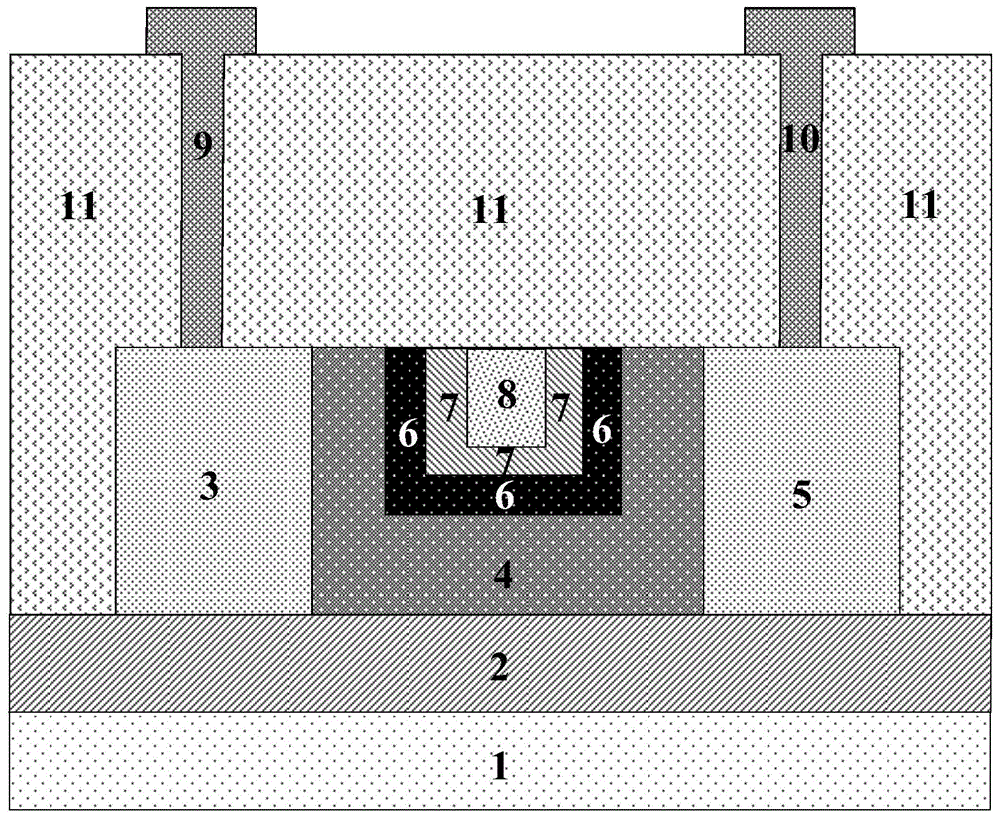
[0045] Such as figure 1 It is a schematic diagram of a two-dimensional structure of an embedded gate insulation tunneling enhanced transistor with high transfer characteristics and low parasitic capacitance in the present invention formed on a bulk silicon substrate; it specifically includes a single crystal silicon substrate 1; a wafer insulating layer 2; an emitter region 3; Region 4; Collector region 5; Conductive layer 6; Tunneling insulating layer 7; Gate electrode 8; Emitter 9; Collector 10;

[0046] High transfer characteristics and low parasitic capacitance Embedded gate insulation tunneling enhancement transistor, using a bulk silicon wafer containing only a single crystal silicon substrate 1 as the device substrate, or using a single crystal silicon substrate 1 and a wafer insulating layer at the same time 2 of the SOI wafer as the substrate for generating devic...


PUM


Abstract

The invention relates to a high-transfer-characteristic low-stray-capacitance embedded grid insulation tunneling enhanced transistor. Compared with MOSFETs or TFETs of the same size as the high-transfer-characteristic low-stray-capacitance embedded grid insulation tunneling enhanced transistor, the better transfer characteristic is achieved by means of the extremely sensitive mutual relation between the impedance of a tunneling insulation layer and the electric field intensity inside the tunneling insulation layer; the problem that stray capacitance among a grid source, a source grid, a grid drain and a drain grid is obviously increased due to the fact that the distance between a grid electrode and a drain electrode or the distance between the grid electrode and a source electrode is gradually decreased is solved; the high transfer characteristic of a device is ensured, and meanwhile the stray capacitance is obviously reduced; due to the fact that no grid-drain overlay area arranged on the MOSFETs or TFETs exists, no obvious reverse leakage current will be caused. The invention further provides a specific manufacturing method of the high-transfer-characteristic low-stray-capacitance embedded grid insulation tunneling enhanced transistor. The high-transfer-characteristic low-stray-capacitance embedded grid insulation tunneling enhanced transistor obviously improves the working characteristic of a nanoscale integrated circuit unit, and is applicable to application and popularization.

Description

Technical field: [0001] The invention relates to the field of ultra-large-scale integrated circuit manufacturing, and relates to an embedded gate insulation tunneling enhanced transistor with high transfer characteristics and low parasitic capacitance, which is suitable for the manufacture of high-performance ultra-high integrated integrated circuits. Background technique: [0002] Currently, the ever-shortening device channel lengths of integrated circuit unit metal-oxide-semiconductor field-effect transistors (MOSFETs) have resulted in degraded device transfer characteristics. The subthreshold swing increases with decreasing channel length, and the static power consumption increases significantly. Although the degradation of the device performance can be alleviated by improving the structure of the gate electrode, when the device size is further reduced, the transfer characteristics of the device will deteriorate again. [0003] On the other hand, with the continuous redu...

Claims


Application Information

Patent Timeline
Patent Type & Authority Applications(China)
IPC IPC(8): H01L29/739H01L29/423H01L29/10H01L21/28H01L21/331
CPCH01L21/28H01L29/0684H01L29/4236H01L29/66931H01L29/739
Inventor 靳晓诗刘溪
Owner SHENYANG POLYTECHNIC UNIV
Why Eureka
Try Eureka