LED epitaxial structure and method achieving high luminous energy density output

An epitaxial structure and density technology, applied in electrical components, circuits, semiconductor devices, etc., can solve problems such as sacrificing efficiency and increasing driving current, achieving good flexibility, high energy conversion efficiency, and improving optical control factors.

Inactive Publication Date: 2015-03-25
江苏鑫博电子科技有限公司
View PDF4 Cites 6 Cited by
  • Summary
  • Abstract
  • Description
  • Claims
  • Application Information

AI Technical Summary

Problems solved by technology

In order to obtain higher photon energy density, lighting fixtures manufactured under the tr...

Method used


Image

  • LED epitaxial structure and method achieving high luminous energy density output
  • LED epitaxial structure and method achieving high luminous energy density output
  • LED epitaxial structure and method achieving high luminous energy density output

Examples


Embodiment Construction

[0046] The principles and features of the present invention are described below in conjunction with the accompanying drawings, and the examples given are only used to explain the present invention, and are not intended to limit the scope of the present invention.

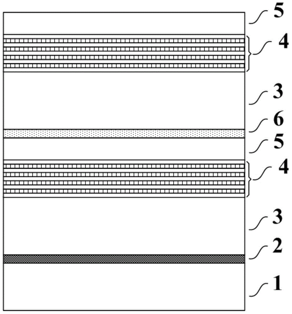
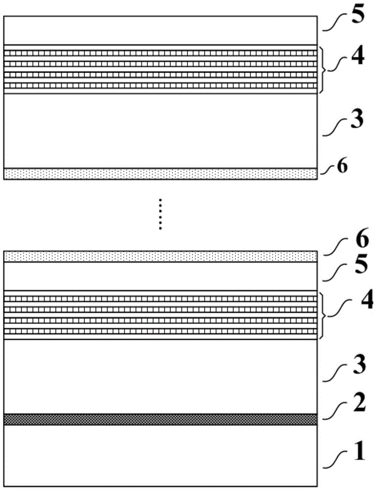
[0047] Such as figure 1 As shown, it is a schematic cross-sectional view of an LED epitaxial structure with high luminous energy density output according to Embodiment 1 of the present invention, including a substrate layer 1, a buffer layer 2, a tunnel node 6 and two groups of LED basic structural units arranged in sequence; The first group of LED basic structural units are respectively composed of n-type layer 3, p-type layer 5 and light-emitting layer 4, the light-emitting layer 4 is located between n-type layer 3 and p-type layer 5; the second group of LED basic structural units are respectively composed of The n-type layer 3 , the p-type layer 5 and the light-emitting layer 4 are formed, and the light-emitting ...


PUM


Abstract

The invention relates to an LED epitaxial structure and method achieving high luminous energy density output. Two or more LED basic structure units are connected in a tunnel segment mode to form a uniform epitaxial device structure. Each LED basic structure unit comprises an n-type layer, a luminous layer and a P-type layer, wherein the luminous layer is located between the n-type layer and the P-type layer, and the n-type layer, the luminous layer and the P-type layer are each composed of multiple sublayers. The LED epitaxial structure can obtain high photonic energy flux density output under low current density injection, so that optical control factors of the device are increased, the problem of efficiency droop of the LED device under high current density drive is relieved, and high energy conversion efficiency of the device is maintained.

Description

technical field [0001] The invention relates to an LED epitaxy structure and an epitaxy method with high light energy density output, and belongs to the field of manufacturing LED optoelectronic devices. Background technique [0002] Based on arsenide Al x In y Ga 1-x-y As(0≤x,y≤1; x+y≤1), phosphide Al x In y Ga 1-x-y P(0≤x,y≤1; x+y≤1), phosphorus arsenide Al x In y Ga 1-x-y As 1-z P z (0≤x,y,z≤1; x+y≤1) and nitride Al x In y Ga 1-x-y N (0≤x, y≤1; x+y≤1; wurtzite crystal structure) light-emitting diode LEDs made of semiconductor materials are gradually being used in electronic display screens, landscape lighting, miner's lamps, and street lamps due to their advantages in energy saving, environmental protection, and long life. , liquid crystal display backlight, general lighting, optical disc information storage, biomedicine and other fields are widely used. The above-mentioned compound semiconductors can cover the entire spectral energy range from infrared, vis...

Claims


Application Information

Patent Timeline
IPC IPC(8): H01L33/06
CPCH01L33/06H01L33/005H01L33/0062H01L33/0075H01L33/02H01L2933/0008H01L2933/0066
Inventor 马亮裴晓将李金权刘素娟胡兵
Owner 江苏鑫博电子科技有限公司
Why Eureka
Try Eureka