
Integrated photoelectrical waveguide modulator with high efficient heat radiation structure and manufacturing method thereof

A technology of waveguide modulator and heat dissipation structure, which is applied in the field of laser communication, can solve the problems of cumbersome and complicated process and high requirements for the design of the new structure of the modulator, and achieve the effects of simple process, thermal drift suppression, and efficient heat dissipation

Inactive Publication Date: 2015-04-01
BEIJING RES INST OF TELEMETRY +1
View PDF2 Cites 2 Cited by
  • Summary
  • Abstract
  • Description
  • Claims
  • Application Information

AI Technical Summary

Problems solved by technology

The former needs to adopt different process flows for different structures of the crystal, and the process is cumbersome and complicated; the latter has higher requirements for the design of the new structure of the modulator

Method used


Image

  • Integrated photoelectrical waveguide modulator with high efficient heat radiation structure and manufacturing method thereof
  • Integrated photoelectrical waveguide modulator with high efficient heat radiation structure and manufacturing method thereof

Examples


Embodiment

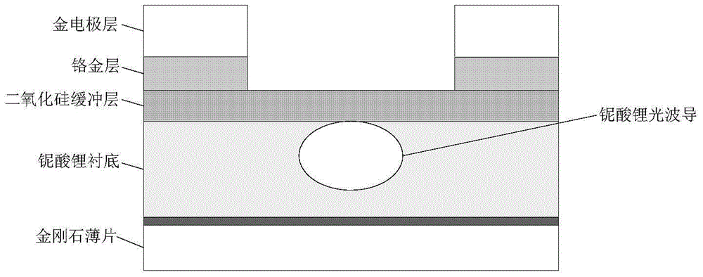
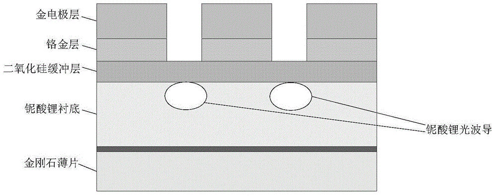
[0035] The size of the lithium niobate crystal selected in this embodiment is 40mm×10mm×2mm, the size of the diamond sheet is 40mm×10mm×1mm, the width of the lithium niobate optical waveguide in the electro-optic waveguide modulator component is 5-8 μm, gold The total thickness of the electrode layer and the chrome-gold layer is 6-15 μm.

[0036] In this embodiment, the specific implementation steps of preparing the integrated electro-optic waveguide modulator are given, including the steps of preparing the components of the electro-optic waveguide modulator and the steps of adding a heat dissipation structure, as follows:

[0037] (1), select an x-cut lithium niobate wafer with a size of 40mm×10mm×2mm;

[0038] (2), successively use absolute ethanol, acetone, trichlorethylene and deionized water to clean the wafer;

[0039] (3) After cleaning the wafer, use a pure nitrogen spray gun to blow the wafer, and the blowing direction of the air flow starts from the center of the wa...


PUM

PropertyMeasurementUnit
thicknessaaaaaaaaaa
thicknessaaaaaaaaaa

Abstract

The invention provides an integrated photoelectrical waveguide modulator with a high-efficient heat radiation structure and a manufacturing method thereof. The integrated photoelectrical waveguide modulator adopts the high-efficient heat radiation structure, the diamond is used as the heat radiation material of lithium niobate substrate, and the liquid capillary bonding is used for achieving the good contact between the lithium niobate substrate and the diamond slice, the thermal resistance and optical loss are not generated, the high heat conductivity feature of the diamond is used for achieving the internal heat radiation of the photoelectrical waveguide modulator, and the internal thermal field of the modulator is uniformed distributed. The integrated photoelectrical waveguide modulator with the high-efficient heat radiation structure has the advantages of simple structure, simple technology, low cost and the like, and can be widely applied to the fields, such as laser communication, optical fiber sensing and optical signal processing.

Description

technical field [0001] The invention belongs to the technical field of laser communication, and relates to an integrated electro-optical waveguide modulator with a high-efficiency heat dissipation structure and a preparation method thereof. Background technique [0002] The integrated electro-optic waveguide modulator is the key device to realize the electro-optic modulation in the laser communication system, and the basis of the modulation is the electro-optic effect of the crystal medium. In the electro-optic waveguide modulator, the linear electro-optic effect of the applied electric field causes the refractive index of the optical waveguide medium to change, which in turn causes the phase change of the guided light propagation. Integrated electro-optic waveguide modulators usually use lithium niobate (LiNbO 3 ) crystal as the substrate. However, in practical applications, the temperature change due to the thermoelectric effect of the electro-optical waveguide modulator...

Claims


Application Information

Patent Timeline
Patent Type & Authority Applications(China)
IPC IPC(8): G02F1/035
CPCG02F1/035
Inventor 刘向南张靓于征谌明向程勇卢满宏杜中伟李英飞
Owner BEIJING RES INST OF TELEMETRY
Learn More