Method for manufacturing smooth polycrystalline silicon film and array substrate

A technology of polysilicon and polysilicon layer, which is applied in semiconductor/solid-state device manufacturing, electrical components, electric solid-state devices, etc. It can solve the problems of liquid crystal display quality degradation, thin-film transistor failure, etc., achieve small surface roughness, improve quality, and eliminate partial The effect of too much electric field

Active Publication Date: 2015-04-01
TCL CHINA STAR OPTOELECTRONICS TECH CO LTD
View PDF3 Cites 9 Cited by
  • Summary
  • Abstract
  • Description
  • Claims
  • Application Information

AI Technical Summary

Problems solved by technology

Generally, it is considered that the polysilicon layer formed by melting and crystallizing the amorphous silicon (ie a-Si) layer will have fine bulges at the grain boundaries, and these bulges are considered to be harmful, because the bulges are very easy to cause thin film transistors. The local electric field is too large to cause the thin film transistor to fail, and cause the quality of the liquid crystal display to be seriously degraded

Method used


Image

  • Method for manufacturing smooth polycrystalline silicon film and array substrate
  • Method for manufacturing smooth polycrystalline silicon film and array substrate
  • Method for manufacturing smooth polycrystalline silicon film and array substrate

Examples


Embodiment 1

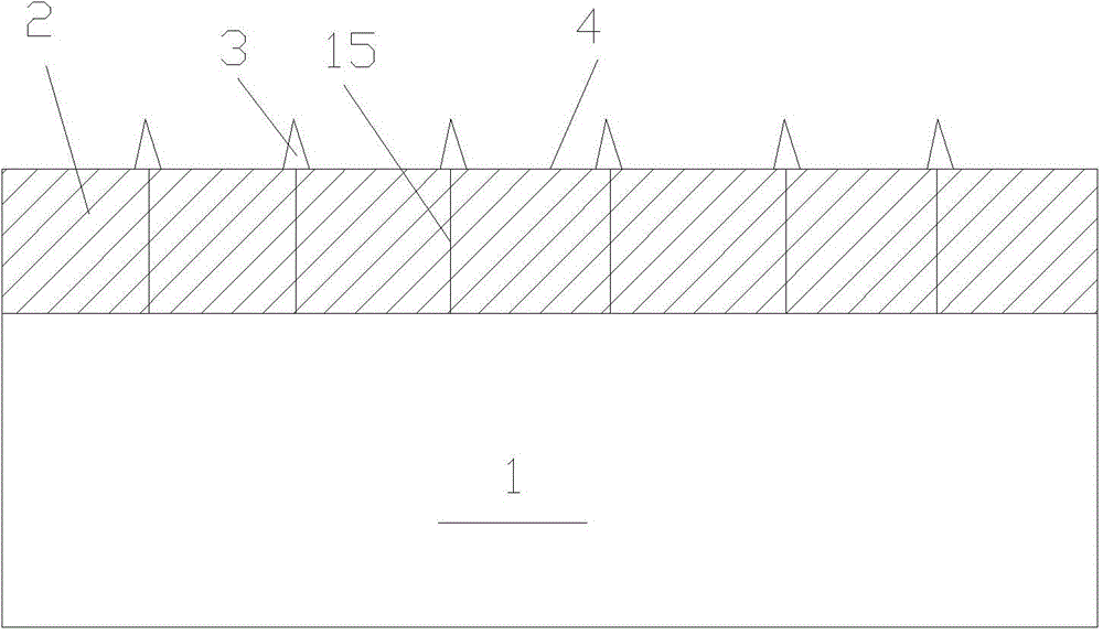
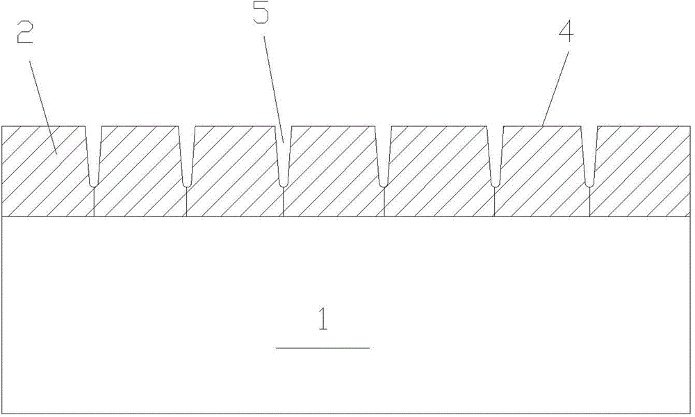
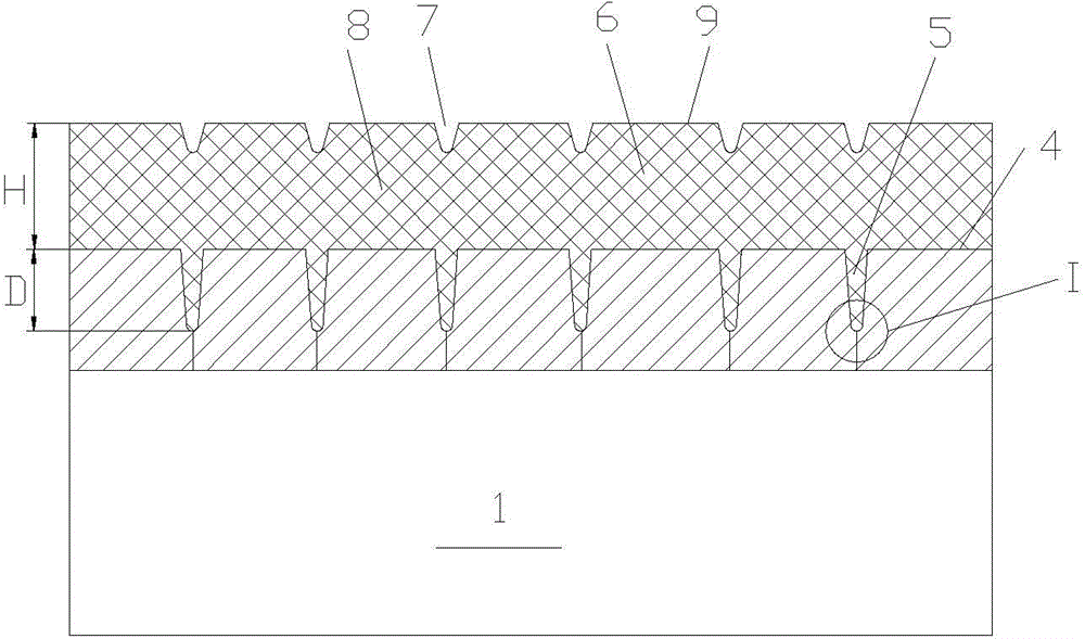
[0032] A first polysilicon layer having a thickness of 450 angstroms was formed on a glass substrate, and a plurality of bumps were formed on the surface of the first polysilicon layer. It is detected that the surface roughness of the flat surface of the first polysilicon layer is 100-150 angstroms. The glass substrate 1 was immersed in a secco etching solution, and etched until there were no bumps but pits on the surface of the first polysilicon layer. The detection found that the depth D of the pit was about 300 angstroms. Next, a second amorphous silicon layer is formed on the surface of the first polysilicon layer. The thickness H of the second amorphous silicon layer is about 500 angstroms, and the second amorphous silicon layer includes a recessed filled region corresponding to the pit and a non-filled region surrounding the filled region. Next, use 420mJ / cm 2 The laser heats the second amorphous silicon layer until the material in the filled area is completely melted...

Embodiment 2

[0034] A first polysilicon layer having a thickness of 450 angstroms was formed on a glass substrate, and a plurality of bumps were formed on a flat surface of the first polysilicon layer. It is detected that the surface roughness of the flat surface of the first polysilicon layer is 100-150 angstroms. use SF 6 with Cl 2 The mixed gas used as an etching medium etches the glass substrate 1 until there are pits instead of bumps on the surface of the first polysilicon layer. The detection found that the depth D of the pit was about 300 angstroms. Next, a second amorphous silicon layer is formed on the surface of the first polysilicon layer. The thickness H of the second amorphous silicon layer is about 500 angstroms, and the second amorphous silicon layer includes a recessed filled region corresponding to the pit and a non-filled region surrounding the filled region. Next, turn the glass substrate 90 degrees with the normal line of the glass substrate as the axis, and then us...


PUM

PropertyMeasurementUnit
thicknessaaaaaaaaaa
depthaaaaaaaaaa
thicknessaaaaaaaaaa

Abstract

The invention relates to a method for manufacturing a smooth polycrystalline silicon film and an array substrate. The method comprises the steps that firstly, a first polycrystalline silicon layer is formed on a substrate, and a plurality of protrusions are arranged on the surface of the first polycrystalline silicon layer; secondly, the surface of the first polycrystalline silicon layer is etched, and the protrusions are etched into pits; thirdly, a second amorphous silicon layer is formed on the surface of the first polycrystalline silicon layer and comprises concave filling areas corresponding to the pits and non-filling areas surrounding the filling areas; fourthly, heat treatment is carried out on the second amorphous silicon layer, the second amorphous silicon layer is crystallized, and protrusions are formed in the concave filling areas to fill and level up the concave filling areas to form a second polycrystalline silicon layer with the smooth surface. The surface roughness of the polycrystalline silicon film manufactured through the method is small, the thickness of a grid insulation layer can be reduced, and therefore power consumption of a liquid crystal displayer is reduced.

Description

technical field [0001] The invention relates to the field of liquid crystal display, in particular to a method for preparing a smooth polysilicon film. Background technique [0002] In the prior art, LTPS TFT liquid crystal displays (i.e. field-effect thin film transistor liquid crystal displays) are widely used in mobile display products due to their good brightness, high contrast, strong layering and bright colors. [0003] In the preparation process of this liquid crystal display, it is necessary to prepare a polysilicon film layer on a glass substrate, and then prepare a thin film transistor by means of the polysilicon film layer. Generally, it is considered that the polysilicon layer formed by melting and crystallizing the amorphous silicon (ie a-Si) layer will have fine bulges at the grain boundaries, and these bulges are considered to be harmful, because the bulges are very easy to cause thin film transistors. The local electric field of the thin film transistor is t...

Claims


Application Information

Patent Timeline
Patent Type & Authority Applications(China)
IPC IPC(8): H01L21/02H01L21/336H01L27/02
CPCH01L21/02H01L21/30604H01L21/3065H01L21/324H01L27/12H01L27/1214
Inventor 胡国仁
Owner TCL CHINA STAR OPTOELECTRONICS TECH CO LTD
Why Eureka
Try Eureka