Manufacturing method of biological neural synapsis bionic electronic devices and products thereof

A technology of neural synapses and electronic devices, applied in the direction of electrical components, specific application simulation processes, etc., can solve the problems of synaptic device units not realizing ultra-low energy consumption operation, etc., to facilitate large-scale integration, improve microstructure and corresponding Effects of electrical performance, ultra-low power operation

Inactive Publication Date: 2015-04-15
NINGBO INST OF MATERIALS TECH & ENG CHINESE ACADEMY OF SCI
View PDF5 Cites 5 Cited by
  • Summary
  • Abstract
  • Description
  • Claims
  • Application Information

AI Technical Summary

Problems solved by technology

The patent documents with publication numbers CN103078054A and CN103078055A disclose the unit and preparation method of the simulated biological synapse based on chalcogenide compounds, but the synapse device unit does not realize ultra-low energy consumption operation

Method used


Image

  • Manufacturing method of biological neural synapsis bionic electronic devices and products thereof
  • Manufacturing method of biological neural synapsis bionic electronic devices and products thereof
  • Manufacturing method of biological neural synapsis bionic electronic devices and products thereof

Examples


Embodiment 1

[0036] The preparation method of the neurosynaptic bionic electronic device unit of the present embodiment includes the following steps:

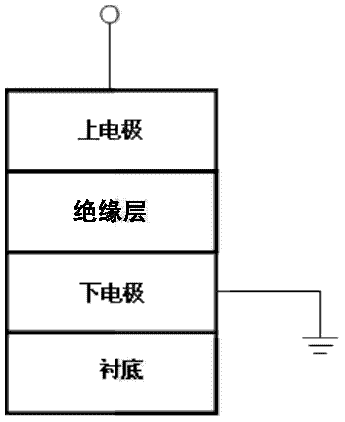
[0037] Step 1. Prepare a 20nm thick titanium thin film and a 150nm thick platinum thin film sequentially on the surface of the substrate as a conductive layer by sputtering.

[0038] In this embodiment, the substrate is a thermally oxidized silicon wafer, and a silicon dioxide isolation dielectric layer is grown on the single crystal silicon to form a thermally oxidized silicon wafer as an insulating substrate. A conductive layer is formed on one side of the silicon dioxide layer of the thermally oxidized silicon wafer.

[0039] Among them, the 20nm thick titanium film is used as a buffer layer, and its main function is to increase the mechanical bonding force between the platinum film and the thermally oxidized silicon wafer.

[0040] Step 2, using magnetron sputtering to prepare a ZnO film with a thickness of 300nm as an insulating film....

Embodiment 2

[0049] Same as Example 1, the difference is that the thickness of the ZnO film prepared in step 2 is 15nm, the amplitude of the first pulse (positive pulse) applied in step 4 is 0.8V, and the second pulse (negative pulse) The amplitude is 0.2V.

[0050] Correspondingly, the difference between the bionic synapse bionic electronic device prepared in this example and Example 1 is that the thickness of the ZnO film in the middle layer is 15 nm, and the pulse voltage used in step 4 is different.

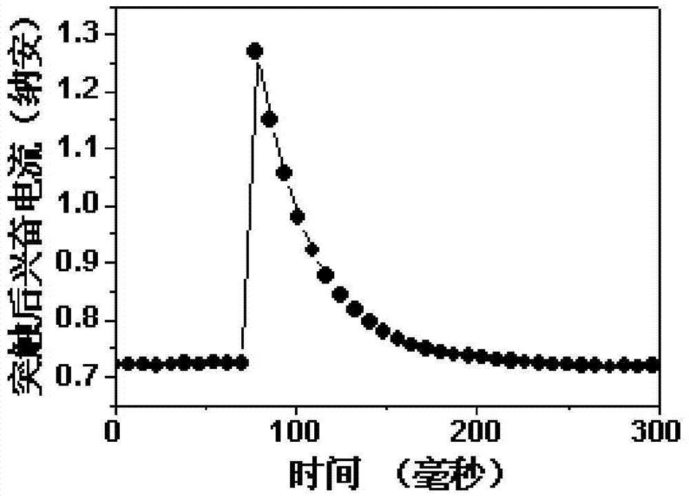
[0051] For the Cu / ZnO / Pt stack structure processed by the two-step voltage method, apply a forward pulse voltage with an amplitude of 5mV and a width of 10ns, and use a voltage of 1mV to read the current value in real time. image 3 This is the relationship between the post-synaptic excitatory current changing with time. It can be seen that under the excitation of a positive pulse voltage with an amplitude of 5mV and a width of 10ns, the device current reaches a peak of 1.3nA, and then d...

Embodiment 3

[0053] Same as Example 1, except that the electrically insulating film prepared in step 2 is amorphous carbon (a-C) with a thickness of 10 nm, the sputtering target is graphite, and the sputtering atmosphere is nitrogen or a mixed gas of nitrogen and argon. The amplitude of the first pulse (positive pulse) applied in step 4 is 3V, and the amplitude of the second pulse (negative pulse) is 0.5V.

[0054] Correspondingly, the difference between the bionic synapse bionic electronic device prepared in this example and Example 1 is that the middle layer is an a-C film with a thickness of 10 nm, and the pulse voltage used in step 4 is different.

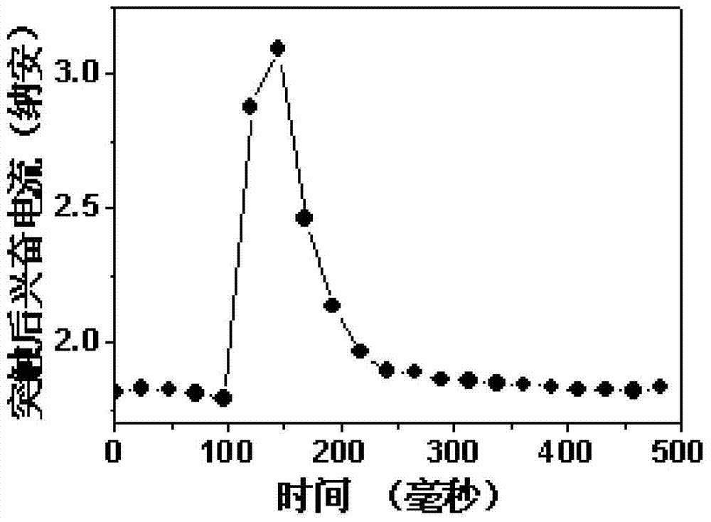
[0055] For the Cu / a-C / Pt stack structure processed by the two-step voltage method, apply a forward pulse voltage with an amplitude of 10mV and a width of 100ns, and use a voltage of 1mV to read the current value in real time. Figure 4 This is the relationship between the post-synaptic excitatory current changing with time. It can be seen ...


PUM


Abstract

The invention discloses a manufacturing method of biological neural synapsis bionic electronic devices and products thereof. The manufacturing method includes (1) sequentially forming a conductive layer and an insulation layer on a substrate; (2) forming a plurality of upper electrodes which are mutually isolated on the insulation layer; (3) grounding the conductive layer, applying first pulse on the upper electrodes and applying second pulse on the upper electrodes; (4) etching the conductive layer and the insulation layer to remove the area not covered by the upper electrodes to obtain the biological neural synapsis bionic electronic devices which are isolated mutually. By subjecting the electrodes / electric insulation films / electrode lamination structures to two-step voltage treatment, microstructure and electric performance of the insulation layer are improved, and when the manufactured biological neural synapsis bionic electronic devices simulate biological neural synapsis function, energy consumption of single synapsis can be lowered to 10-5 fj, so that ultralow energy consumption is realized, and massive integration of the biological neural synapsis bionic electronic devices is facilitated.

Description

technical field [0001] The invention relates to the technical field of microelectronic devices, in particular to a preparation method and a product of a bionic synapse bionic electronic device. Background technique [0002] Memristor has a very simple metal / dielectric layer (ie middle layer) / metal stack structure, and is the fourth basic passive electronic device besides resistors, capacitors, and inductors. As early as 1971, Cai Shaotang, a Chinese electronic engineer at the University of California, Berkeley, predicted that through theoretical calculations, there must be a fourth passive electronic component besides resistors, capacitors and inductors. 37 years later (2008), the United States Hewlett-Packard Company announced that in Pt / TiO 2–x Find this missing circuit element in the device at both ends of / Pt. The memristor has the dimension of resistance, but it has nonlinear electrical properties different from ordinary resistors. Its resistance value will change wit...

Claims


Application Information

Patent Timeline
Patent Type & Authority Applications(China)
IPC IPC(8): H01L45/00G06G7/60
Inventor 诸葛飞潘若冰曹鸿涛竺立强李俊
Owner NINGBO INST OF MATERIALS TECH & ENG CHINESE ACADEMY OF SCI
Why Eureka
Try Eureka