Device and method for directly growing atom-dimension two-dimensional semiconductor heterojunction

A two-dimensional semiconductor and heterojunction technology, applied in the fields of mechanical manufacturing and material science and engineering, can solve the problems of device consistency, difficulty in ensuring repeatability, affecting material device performance, and cumbersome transfer process, so as to shorten the time for material growth , increase the preparation time, and ensure the effect of successful growth

Active Publication Date: 2015-04-22
HARBIN INST OF TECH
View PDF4 Cites 13 Cited by
  • Summary
  • Abstract
  • Description
  • Claims
  • Application Information

AI Technical Summary

Problems solved by technology

With this method, there is only a weak van der Waals force between the two materials, and the carriers will be severely scattered at the interface, which will affect the performance of the material device.
At the same time, impurities a

Method used


Image

  • Device and method for directly growing atom-dimension two-dimensional semiconductor heterojunction
  • Device and method for directly growing atom-dimension two-dimensional semiconductor heterojunction
  • Device and method for directly growing atom-dimension two-dimensional semiconductor heterojunction

Examples


specific Embodiment approach 1

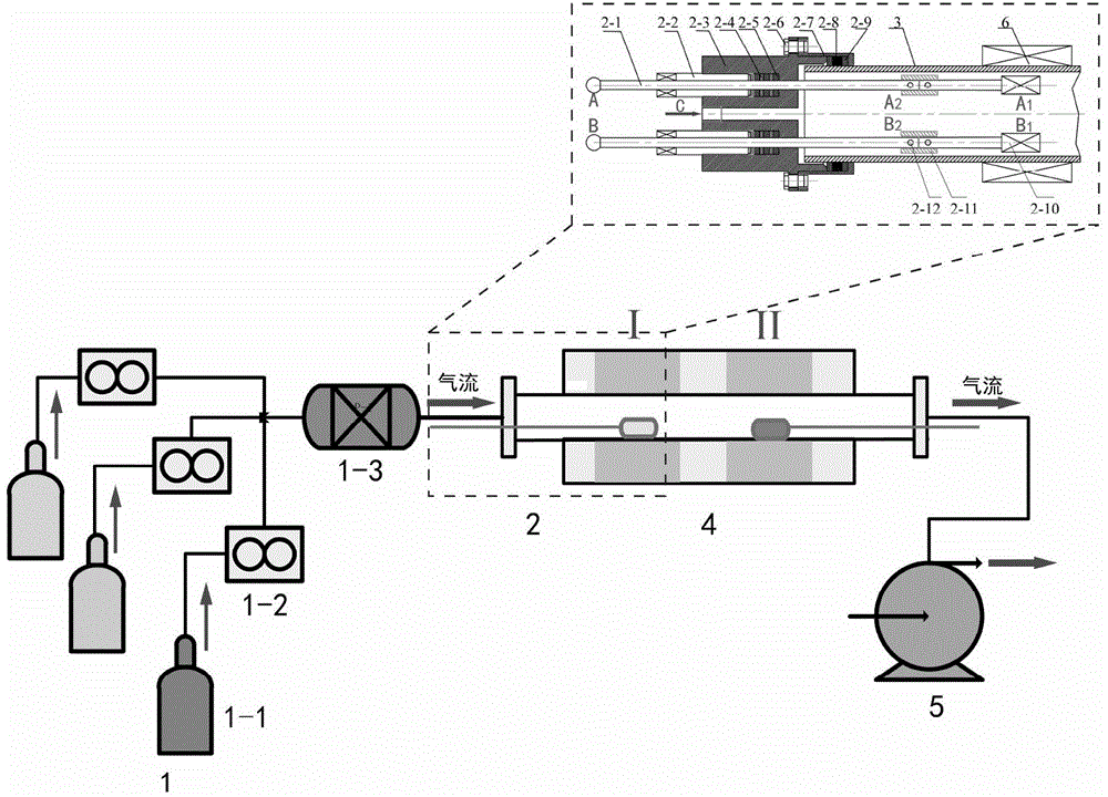
[0031] Specific implementation mode one: as figure 1 As shown, this embodiment provides a device for directly growing an atomic-scale two-dimensional semiconductor heterojunction, which mainly includes five parts: an atmosphere adjustment device 1, a fast switching device 2, a quartz tube 3, a heating device 4, and a vacuum adjustment device 5. Among them, the fast switching device 2 is a key component to ensure the successful preparation of an atomic-scale two-dimensional semiconductor heterojunction.

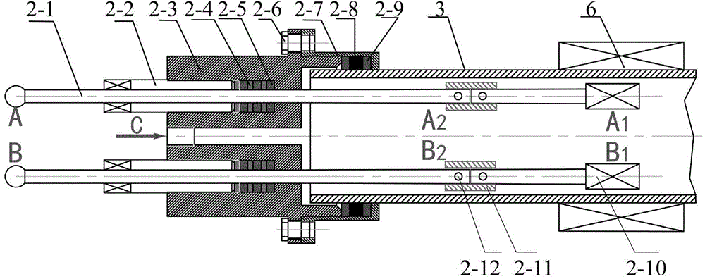
[0032] Such as figure 2 As shown, the quick switching device 2 includes a precursor switching rod 2-1 located at the left end of the quartz tube, a substrate switching rod located at the right end of the quartz tube (the structure is exactly the same as 2-1), a sealing screw 2-2, and a rear end cover 2- 3. Screws 2-6, front end cover 2-7, first sleeve 2-4, second sleeve 2-8, first high temperature resistant O-ring 2-5, second high temperature resistant O-ring 2-9, quartz Co...

specific Embodiment approach 2

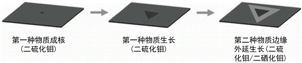
[0055]Specific Embodiment 2: Taking two precursor switching rods A, B and one substrate switching rod as examples to illustrate the growth process of the heterojunction of two materials. First, place the reaction precursor and the substrate in the reaction chamber. Typically, the precursor is placed on a quartz member connected to the precursor switching rod, and the substrate is placed on the quartz member connected to the substrate switching rod. In some cases, there are more than one kind of precursors used to grow a substance, and it is necessary to place some substances next to the quartz member on the right end of the quartz tube where the substrate is placed. It reacts with the precursors brought by the carrier gas and forms the desired substance on the substrate. substance. For example, the reaction of using sulfur powder and molybdenum trioxide powder to grow molybdenum disulfide on a silicon substrate. The sulfur powder is placed on the quartz member of the switchin...

specific Embodiment approach 3

[0058] Embodiment 3: Taking the growth of a molybdenum disulfide / molybdenum diselenide heterojunction as an example, a specific implementation method for directly growing an atomic-scale two-dimensional semiconductor heterojunction is described.

[0059] 1. Using molybdenum trioxide as molybdenum source, elemental sulfur powder and elemental selenium powder as precursors, grow molybdenum disulfide / molybdenum diselenide heterojunction on the substrate.

[0060] 2. Molybdenum trioxide, elemental sulfur powder and selenium powder are commercial products with a purity of 99.9-99.999%, without purification or other treatment before use. The substrate can be a silicon wafer with a silicon dioxide layer, a quartz wafer, a mica wafer, hexagonal boron nitride, etc., and the thickness of the oxide layer of the silicon wafer with a silicon dioxide layer can be 50-500 nm. The purity of molybdenum trioxide is 98-99.99%.

[0061] 3. Place molybdenum trioxide as the molybdenum source on the...


PUM

PropertyMeasurementUnit
Outer diameteraaaaaaaaaa

Abstract

The invention discloses a device and method for directly growing atom-dimension two-dimensional semiconductor heterojunction. The device comprises an atmosphere adjusting device, rapid switching devices, a quartz tube, a heating device and a vacuum adjusting device. The middle section of the quartz tube is located inside the heating device, the rapid switching devices are arranged at the left and right ends of the quartz tube, and comprise switching rods, rear end covers, front end covers, first sleeves, second sleeves, first high-temperature-resistant O rings, second high-temperature-resistant O rings and quartz components. The device has the advantages of being efficient, rapid and simple in structure, and through the reaction device, the atom-dimension two-dimensional semiconductor heterojunction can be directly grown on the surface of a substrate. The device can be used for growing the heterojunction or two or more kinds of single substances through one-time reaction, in this way, the growing time of the material is shortened, the growing cost is lowered, and production efficiency is improved.

Description

technical field [0001] The invention belongs to the technical fields of mechanical manufacturing and material science engineering, and relates to a device and method for directly growing an atomic-scale two-dimensional semiconductor heterojunction. Background technique [0002] Two-dimensional materials are an important class of materials that have only been developed in the last ten years. Their thickness usually ranges from a fraction of a nanometer to tens of nanometers, and their planar dimensions range from tens of nanometers to hundreds of meters. They span microscopic, mesoscopic and macroscopic Three scales. Due to the nanoscale scale in a certain dimension, two-dimensional materials have many excellent physical and chemical properties, such as the quantum size effect of two-dimensional materials, the quantum confinement effect, the plane transport of carriers, and the surface of the material without suspension. Bonds, the atoms that make up the material are concent...

Claims


Application Information

Patent Timeline
IPC IPC(8): H01L21/04H01L21/67B82Y40/00
CPCB82Y40/00H01L21/04H01L21/67011
Inventor 胡平安张甲陈晓爽郑威冯伟刘光波
Owner HARBIN INST OF TECH
Why Eureka
Try Eureka