Thin film transistor, manufacturing method of thin film transistor, array substrate and display device

A technology of thin film transistors and manufacturing methods, which is applied in the direction of transistors, semiconductor/solid-state device manufacturing, semiconductor devices, etc., can solve problems such as complex manufacturing processes and increased manufacturing costs, and achieve the goal of reducing quantity, reducing defect state density, and improving stability Effect

Inactive Publication Date: 2015-04-22
BOE TECH GRP CO LTD
View PDF7 Cites 9 Cited by
  • Summary
  • Abstract
  • Description
  • Claims
  • Application Information

AI Technical Summary

Problems solved by technology

However, these methods increase the production cost and complicate the production process.

Method used


Image

  • Thin film transistor, manufacturing method of thin film transistor, array substrate and display device

Examples


Embodiment approach

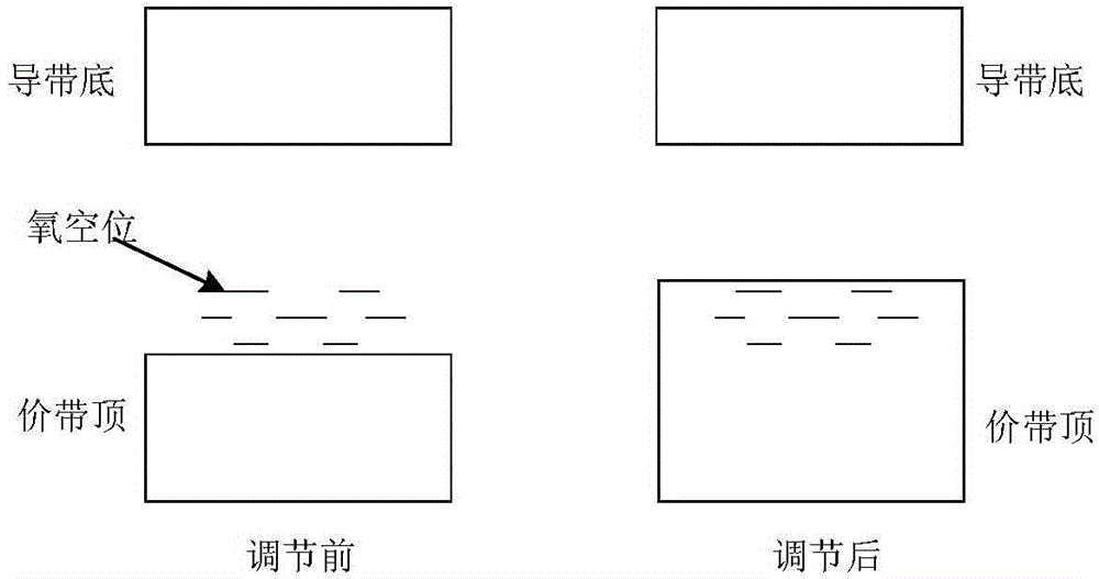
[0032] As a specific embodiment of the present invention, the oxide includes zinc oxide, and the dopant ions include N 3- or S 2- , the molar ratio of the dopant ions to the total amount of oxygen ions in the oxide is between 5% and 80%, which can be regarded as: 5%≤N 3- / (N 3- +O 2- )≤80%, or 5%≤S 2- / (S 2- +O 2- )≤80%. The band gap of zinc oxide is 3.32eV, and the band gaps of zinc nitride and zinc sulfide are both 1.1eV. When the dopant ions include N 3- , the active layer (i.e. doped with N 3-The band gap of the zinc oxide layer) is smaller than the band gap of zinc oxide, and the top of the valence band moves up, thereby reducing the oxygen vacancies Vo; similarly, when the dopant ions include S 2- , the active layer (i.e. doped with S 2- The band gap of the zinc oxide layer) will also be smaller than that of zinc oxide, and the top of the valence band will move up, thereby reducing the oxygen vacancies Vo.

[0033] The thin film transistor includes but is not l...


PUM


Abstract

The invention provides a thin film transistor. The thin film transistor comprises a grid electrode, an active layer, a source electrode and a drain electrode which are formed on a substrate, wherein the active layer contains an ion-doped oxide, doped ions are of p-track electron configuration structures, and the p-track energy level of the doped ions is higher than 2 p-track energy level of oxygen ions in the oxide so as to enable the valence-band top of the active layer after doping to be higher than the energy level of oxygen vacancy formed in the active layer. Correspondingly, the invention further provides a manufacturing method of the thin film transistor, an array substrate and a display device. The active layer of the thin film transistor is mainly made of the ion-doped oxide, the stability of the thin film transistor can be improved, a shading structure is not needed to be added on the display device, and a manufacturing process is simplified.

Description

technical field [0001] The present invention relates to the field of display technology, in particular to a thin film transistor and a manufacturing method thereof, an array substrate including the thin film transistor, and a display device including the array substrate. Background technique [0002] Oxide thin-film transistors have the advantages of good uniformity, transparency, and simple manufacturing process, and their carrier concentration is ten times or even dozens of times that of amorphous silicon. It has attracted much attention in liquid crystal displays and organic light-emitting diode displays. [0003] However, the current oxide thin film transistors represented by indium gallium zinc oxide (IGZO) and indium tin zinc oxide (ITZO) generally have the problem of poor photostability, that is, the threshold voltage of the thin film transistor will be biased under light conditions. shift, and even thin film transistors fail, seriously affecting the mass production a...

Claims


Application Information

Patent Timeline
Patent Type & Authority Applications(China)
IPC IPC(8): H01L29/786H01L21/336H01L21/77
CPCH01L21/77H01L29/36H01L29/66742H01L29/7869H01L21/02565H01L29/24H01L21/02554H01L21/02631H01L29/66969H01L29/786H01L21/383H01L27/1225
Inventor 王美丽
Owner BOE TECH GRP CO LTD
Why Eureka
Try Eureka