Crystalline silicon cell and manufacturing method thereof

A technology of crystalline silicon cells and manufacturing methods, which is applied in the field of solar cells, can solve problems such as low parallel resistance, unfavorable photoelectric conversion efficiency of crystalline silicon solar cells, and enhanced ability to conduct charges, so as to achieve parallel resistance improvement and photoelectric conversion efficiency improvement , the effect of simple method

Active Publication Date: 2015-04-22
ZHEJIANG BEYONDSUN PV
View PDF5 Cites 1 Cited by
  • Summary
  • Abstract
  • Description
  • Claims
  • Application Information

AI Technical Summary

Problems solved by technology

Especially in order to better enable the silicon nitride layer to achieve the dual functions of passivation and anti-reflection, double-layer or multi-layer silicon nitride is usually used, and the underlying silicon nitride multi-layer has a large silicon content, and its ability to conduct charges is greatly improved Strengthening, which will lead to devices with lower parallel resistance, which is not conducive to the photoelectric conversion efficiency of crystalline silicon solar cells

Method used


Image

  • Crystalline silicon cell and manufacturing method thereof
  • Crystalline silicon cell and manufacturing method thereof
  • Crystalline silicon cell and manufacturing method thereof

Examples


Embodiment 1

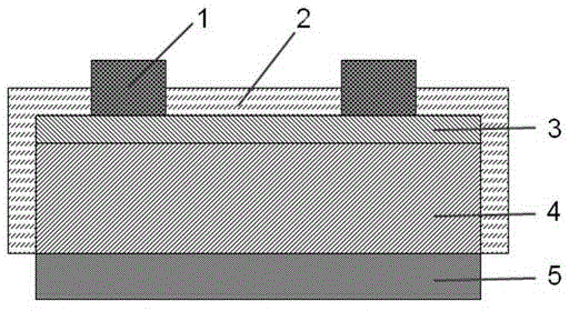
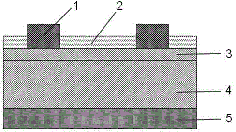
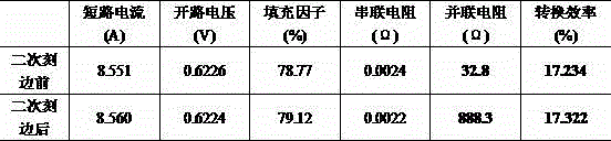
[0023] Embodiment 1: The manufacturing method of the crystalline silicon battery of the embodiment of the present invention, the specific implementation steps are as follows: polysilicon with an area of ​​156*156 is subjected to texturing, diffusion junction, edge cutting, phosphorus silicon glass removal, and silicon nitride anti-reflection deposition Layer, printed electrodes and sintering processes to obtain crystalline silicon solar cells, followed by a second edge-cutting process. Among them, the secondary edge cutting process adopts wet chemical etching, wets the dust-free cloth with 5-10% hydrofluoric acid solution, and then places the edge of the crystalline silicon cell on the dust-free cloth for 15-20 minutes Finally, the color at the edge of the crystalline silicon cell changes from blue to bright gray, and the silicon nitride layer is removed. Table 1 shows the electrical performance parameters of crystalline silicon solar cells before and after the second edge bev...

Embodiment 2

[0026] Embodiment 2: The manufacturing method of crystalline silicon cell, the specific implementation steps are as follows: polycrystalline silicon with an area of ​​156*156 is processed through texturing, diffusion junction, edge cutting, phosphorus silicon glass removal and silicon nitride anti-reflection layer deposition, followed by Secondary edge cutting process. Among them, the secondary edge cutting process adopts wet chemical etching, and the dust-free cloth is wetted in a mixed acid solution with a concentration of 65% nitric acid and a concentration of 5-10% hydrofluoric acid. Among them, the volume ratio of nitric acid to hydrofluoric acid 4:1, then place the edge of the crystalline silicon cell on a dust-free cloth, and after about 10 minutes, the color at the edge of the crystalline silicon cell changes from blue to bright gray, and the silicon nitride layer is removed. Finally, printed electrodes and sintering process to produce crystalline silicon solar cells. ...


PUM


Abstract

The invention provides a crystalline silicon cell and a manufacturing method of the crystalline silicon cell. The method includes the following steps of texture surface making, diffusion junction making, edge etching, phosphorosilicate glass removal, silicon nitride antireflection layer deposition, electrode printing, sintering and test sorting. The secondary edge etching process is introduced in the steps, a silicon nitride layer on the edge of a crystalline silicon cell piece is removed, the parallel resistance of the crystalline silicon cell is increased, and the photoelectric conversion efficiency of the crystalline silicon cell is improved. In addition, the secondary edge etching process can be selectively introduced after the silicon nitride antireflection layer deposition process and the silicon nitride layer on the edge of the cell is removed; or the secondary edge etching process can be selectively introduced after the sintering process and the silicon nitride layer on the edge of the cell is removed. The method is simple, easy to operate and free of limitation to other process steps.

Description

technical field [0001] The invention relates to a crystalline silicon battery and a manufacturing method thereof, belonging to the technical field of solar batteries. Background technique [0002] How to improve the photoelectric conversion efficiency of crystalline silicon solar cells is an important research topic in the field of photovoltaics. According to the equivalent circuit model of crystalline silicon solar cells, its photoelectric conversion efficiency depends on the reverse saturation current, ideality factor, series resistance and parallel resistance of the device. Among them, the larger the parallel resistance is, the more favorable the photoelectric conversion of the device is. The smaller parallel resistance will reduce the device fill factor and open circuit voltage, which will lead to a decrease in the photoelectric conversion capability of the device. [0003] The parallel resistance of crystalline silicon solar cells depends on its entire preparation pro...

Claims


Application Information

Patent Timeline
Patent Type & Authority Applications(China)
IPC IPC(8): H01L31/18H01L31/04H01L31/055
CPCH01L31/0216H01L31/04H01L31/186Y02E10/52Y02P70/50
Inventor 陈作庚吕文辉龚熠
Owner ZHEJIANG BEYONDSUN PV
Why Eureka
Try Eureka