

A semiconductor device with improved current spreading
A technology of current expansion and current expansion layer, which is applied in the field of semiconductor devices to improve current expansion, can solve the problems of device performance degradation, voltage increase, limited conductivity, etc., achieve chip structure design and electrode distribution flexibility, reduce occupied area, Improve the effect of length
- Summary
- Abstract
- Description
- Claims
- Application Information
AI Technical Summary
Problems solved by technology
Method used
Image

Examples
Embodiment 1
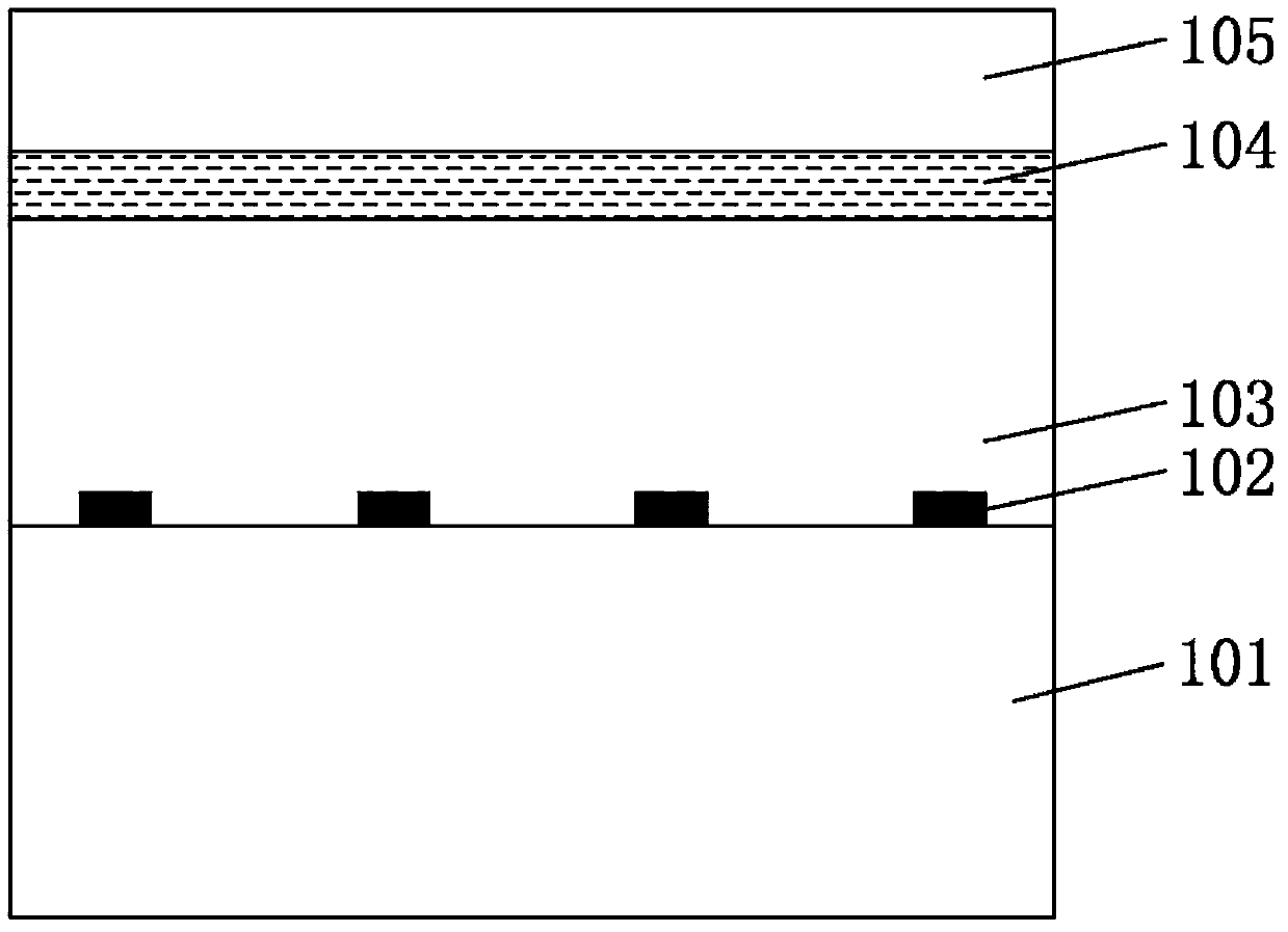
[0040] see Figure 1a , which is a schematic cross-sectional structure diagram of the epitaxial wafer of Embodiment 1 of the improved current spreading LED of the present invention.
[0041] The device includes a substrate 101, on which a metal tungsten mesh grid 102 is arranged, the thickness of the tungsten metal layer is preferably about 10 nanometers to 200 nanometers, the line width of the tungsten metal is about 5 to 10 microns, and the spacing is about 100 μm. ~300 microns, and then grow a GaN buffer layer at a temperature of about 550 degrees, with a thickness of about 30nm, and then grow n-GaN layer 103, InGaN / GaN multiple quantum well layer 104, p-GaN layer 105 and other structures on it. AlGaN layers and the like may also be inserted between the layers. figure 2 It is a three-dimensional schematic diagram of the metal tungsten mesh grid 102 formed on the substrate 101 before epitaxial growth of the device.
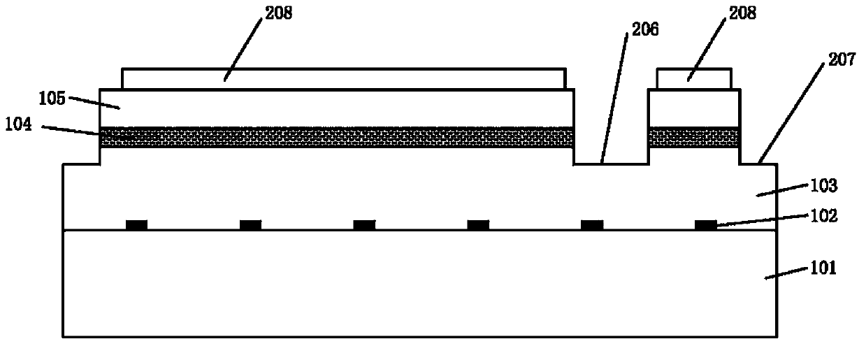
[0042] ginseng Figure 1b shown, through photoresist or ...
Embodiment 2
[0048] Example 2: Similar to Example 1, the only difference is that after growing an epitaxial layer with a certain thickness, the epitaxial wafer is taken out, and the current spreading layer is inserted by deposition or transfer method, and then the epitaxial growth is performed again.
Embodiment 3
[0049] Embodiment 3: its epitaxial structure is also as Figure 1a shown.
[0050] like Figure 6 As shown, a p-GaN mesa is formed by photolithography and etching to expose the n-GaN contact hole 507, and then a p-GaN transparent ohmic contact conductive layer 514 is prepared in the p-GaN mesa region.
[0051] Further, a metal layer 515 and pad metal layer 516 are sequentially deposited and patterned on the n-GaN and p-GaN surfaces. Metal layer 515 forms an ohmic contact on the n-GaN surface and assists current spreading on the p-GaN surface.
[0052] The material of the transparent ohmic contact conductive layer is preferably ITO, NiAu, etc.; the material of the pad metal layer is preferably TiAlTiAu, CrAu, etc.
[0053] Figure 7a is a schematic plan view of the device, Figure 7b is a schematic plan view of the device without inserting the current spreading layer as a comparison. Wherein 617 is a p-GaN mesa region. Compared Figure 7a and Figure 7b It can be seen ...
PUM
 Abstract
Description
Claims
Application Information