Printed circuit board solder mask manufacturing method

A technology for printed circuit boards and manufacturing methods, which is applied in the fields of printed circuit manufacturing, printed circuits, and secondary processing of printed circuits, and can solve problems such as insufficient flatness of solder resist, inconsistent glue flow speed, and wafer cracks, and achieve improved Improve the flatness of the solder mask surface, reduce the production cost, and reduce the effect of solder mask depression

Active Publication Date: 2015-04-22
GUANGZHOU FASTPRINT CIRCUIT TECH +2
View PDF5 Cites 16 Cited by
  • Summary
  • Abstract
  • Description
  • Claims
  • Application Information

AI Technical Summary

Problems solved by technology

[0013] But there are still their own deficiencies, especially for circuit boards (PCB), especially when the chip mounting on the IC packaging substrate requires a high flatness solder mask surface and plug hole quality, the above three new combined processes are difficult At the same time, it meets the customer's product requirements for solder mask flatness and plugging capability. Either the solder mask flatness is not enough, or the solder mask plugging capability is insufficient, such as figure 1 As shown, it is easy to cause wafer cracks and inconsistent glue flow speeds in the subsequent packaging process, which increases the risk of packaging failure and needs to be improved.

Method used


Image

  • Printed circuit board solder mask manufacturing method
  • Printed circuit board solder mask manufacturing method
  • Printed circuit board solder mask manufacturing method

Examples


Embodiment 1

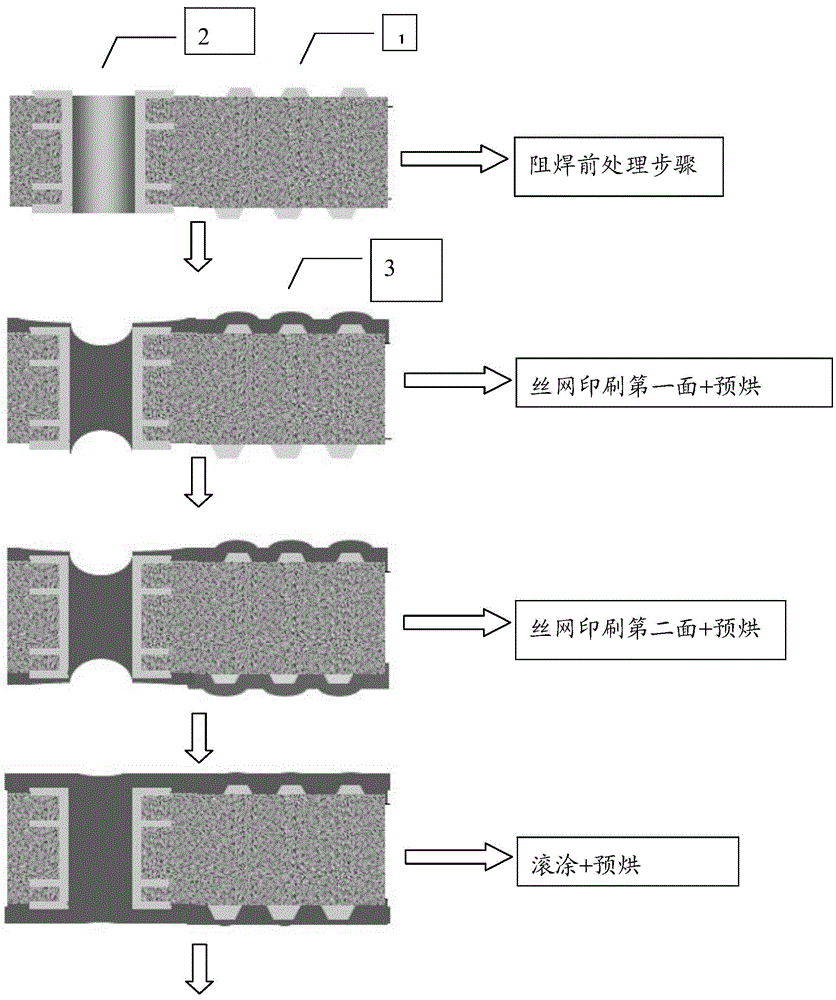
[0044] A method for manufacturing a solder resist on a printed circuit board, wherein the method comprises: a step of screen printing on the first surface, a first pre-baking step, a second screen printing step, a second pre-baking step, and a roll coating step, The third pre-baking step, exposure step, development step, post-curing step.

[0045] The following is based on figure 2 and image 3 As shown, among them, the screen printing first surface step and the first pre-baking step adopt the block screen and backing plate corresponding to the product graphics, and use the scraper to print the surface of the circuit board continuously, which is not only suitable for the needs The position of the plug hole is soldered to plug the hole, and at the same time a thin layer of solder resist is formed on the surface of the circuit board. Among them, in order to prevent the tool hole from being blocked, the upper stop point of the screen plate is increased by 100-200um compared wi...

Embodiment 2

[0052] A method for manufacturing a printed circuit board solder resist, wherein the method includes: a pre-treatment step for solder resist, a step of screen printing on the first side, a first pre-baking step, a step of screen printing on the second side, and a second pre-baking step step, roll coating step, third pre-baking step, exposure step, development step, post-curing step.

[0053] Compared with Example 1, this embodiment adds a solder resist pretreatment step, that is, before printing the solder resist, the surface of the circuit board is treated with a specific physical or chemical method, the purpose of which is to clean the surface of the circuit board And roughening, the amount of micro-etching is controlled at 1±0.2um, so that the solder mask ink has a better bonding force with the surface of the circuit board, and prevents the solder mask from falling off.

Embodiment 3

[0055] A method for manufacturing a printed circuit board solder resist, wherein the method includes: a pre-treatment step for solder resist, a step of screen printing on the first side, a first pre-baking step, a step of screen printing on the second side, and a second pre-baking step step, roll coating step, third pre-baking step, vacuum treatment step, exposure step, development step, post-curing step.

[0056] Compared with Example 1, this embodiment can carry out vacuum pressure treatment on the pre-cured product before exposure, and through the vacuum, leveling and pressing of the vacuum laminator, the solder resist distribution on the surface of the circuit board is more uniform, and the thickness more consistent.


PUM


Abstract

The invention provides a printed circuit board solder mask manufacturing method. The printed circuit board solder mask manufacturing method is characterized by comprising the steps of silk-screen printing of a first side, pre-drying for the first time, silk-screen printing of a second side, pre-drying for the second time, roller coating, pre-drying for the third time, exposing, developing and post-curing. According to the printed circuit board solder mask manufacturing method, on the premise that the requirement for the solder mask thickness of a product is met, solder mask surface smoothness is improved, and the number of solder mask pits is reduced; meanwhile, due to the fact that roller coating is used for double-faced coating and automatic production is adopted, production efficiency is improved, and production cost is reduced.

Description

【Technical field】 [0001] The invention relates to the field of silk screen printing, in particular to a method for manufacturing printed circuit board solder resistance. 【Background technique】 [0002] With the development of electronic products in the direction of light, thin and small, electronic components are also progressing in the direction of high density and miniaturization. Various chip components, especially thin chip components, are placed on circuit boards (PCBs), especially IC packaging substrates. Mounting requires a high flatness solder mask surface. At the same time, due to the development of high-frequency and high-speed signal transmission, a surface solder mask with uniform thickness is also required. However, due to the uneven distribution of solder resist, inconsistent surface thickness, and large depression of solder resist plug holes in the traditional silk screen solder mask process, it is easy to cause wafer cracks and inconsistent glue flow speeds ...

Claims


Application Information

Patent Timeline
Patent Type & Authority Applications(China)
IPC IPC(8): H05K3/28
CPCH05K3/282H05K2203/14
Inventor 陈意铭李志东谢添华
Owner GUANGZHOU FASTPRINT CIRCUIT TECH
Why Eureka
Try Eureka