Silicon carbide wafer bevel grinding, milling and polishing machine and operation method thereof

A technology of silicon carbide crystal and polishing machine, which is applied in the field of grinding and polishing, grinding of silicon carbide wafer bevel, grinding, polishing processing equipment, silicon carbide wafer bevel grinding, which can solve the problem of difficult control of wafer grinding and grinding angle, Problems such as large width dimension error and low polishing processing efficiency can achieve the effect of stable width dimension, high machining accuracy and high work efficiency

Active Publication Date: 2015-04-29
山东粤海金半导体科技有限公司
View PDF5 Cites 34 Cited by
  • Summary
  • Abstract
  • Description
  • Claims
  • Application Information

AI Technical Summary

Problems solved by technology

[0003] 1. The chamfering slope of the wafer has a large width and dimension error after grinding and polishing;
[0004] 2. The chamfering slope of the wafer has poor angle consistency after grinding and polishing;
[0005] 3. The grinding and polishing process of the chamfering slope of the wafer is low in efficiency and high in cost
[0006] 4. It is difficult to control the grinding and grinding angle of the chamfering slope of the wafer, and the error is large

Method used


Image

  • Silicon carbide wafer bevel grinding, milling and polishing machine and operation method thereof
  • Silicon carbide wafer bevel grinding, milling and polishing machine and operation method thereof

Examples


Embodiment 1

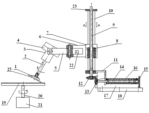
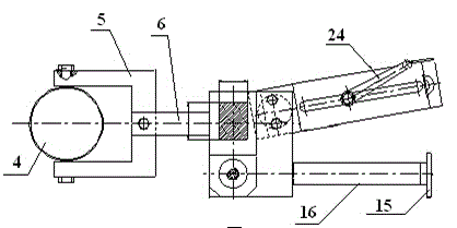
[0035] Such as figure 1 and figure 2As shown, a silicon carbide wafer bevel grinding, grinding and polishing machine, which includes a support piece (1), a rotating shaft (2) connected to the supporting piece (1), and a drive motor connected to the rotating shaft (2) ( 3), the drive motor (3) is installed on the motor bracket (4), the motor bracket (4) is installed on the vertical arm (5), the vertical arm (5) and the horizontal arm (6) ), the horizontal arm (6) is connected with the carriage (7), the carriage (7) is connected with the screw (9) through the inner bushing (8), and the outer periphery of the screw (9) is provided with a bushing (10) , the bushing sleeve (10) is fixed on the column (11), the lower end of the screw rod (9) is connected with the first bevel gear (12), and the first bevel gear (12) is connected with the second bevel gear (13), the The second bevel gear (13) is connected with the adjustment shaft (14), and the adjustment shaft (14) is connected wi...

Embodiment 2

[0044] A circular silicon carbide wafer bevel grinding, lapping and polishing method, which comprises the following steps:

[0045] a. If figure 1 As shown, firstly, the circular silicon carbide wafer (25) to be processed is bonded on the support sheet (1), then the grinding wheel is first installed on the upper end of the shaft (19), and then the motor (20) is started, and the motor (20) drives The grinding wheel on the shaft (19) rotates;

[0046] b. Rotate the runner (14), the runner (14) drives the adjustment shaft (13) to rotate, and then the adjustment shaft (13) drives the second bevel gear (13) and the first bevel gear (12) to rotate in turn, the first bevel gear The gear (12) drives the screw (9) to rotate, and the screw (9) drives the carriage (7) to move up and down, thereby driving the horizontal arm (6) and the vertical arm (5) to move up and down in turn, and then the vertical arm (5) ) to drive the drive motor (3) on the motor bracket (4) to move up and down, ...

Embodiment 3

[0054] Rectangular silicon carbide wafer bevel grinding, grinding and polishing method, it comprises the following steps:

[0055] a. First, bond the rectangular silicon carbide wafer to be processed on the support sheet (1), then install the grinding wheel on the upper end of the shaft (19), then start the motor (20), and the motor (20) drives the shaft (19) wheel rotation;

[0056] b. Rotate the runner (14), the runner (14) drives the adjustment shaft (13) to rotate, and then the adjustment shaft (13) drives the second bevel gear (13) and the first bevel gear (12) to rotate in turn, the first bevel gear The gear (12) drives the screw (9) to rotate, and the screw (9) drives the carriage (7) to move up and down, thereby driving the horizontal arm (6) and the vertical arm (5) to move up and down in turn, and then the vertical arm (5) ) to drive the drive motor (3) on the motor bracket (4) to move up and down, thereby adjusting the distance between the circular silicon carbide ...


PUM

PropertyMeasurementUnit
particle sizeaaaaaaaaaa

Abstract

The invention discloses a silicon carbide wafer bevel grinding, milling and polishing machine and an operation method thereof. The silicon carbide wafer bevel grinding, milling and polishing machine comprises a supporting sheet (1), a rotating shaft (2), a driving motor (3), a motor bracket (4), a vertical rotating arm (5), a horizontal rotating arm (6), a slide frame (7) and a screw rod (9) which are sequentially connected, wherein the lower end of the screw rod (9) is sequentially connected with a first cone gear (12), a second cone gear (13), an adjusting shaft (14) and a rotating wheel (15); a machining tool (19) of a silicon carbide wafer is arranged below the supporting sheet (1). The silicon carbide wafer bevel grinding, milling and polishing machine is reasonable in structural design, convenient to operate and high in working efficiency, bevel grinding, milling and polishing integrated machining can be performed on the silicon carbide wafer, the working efficiency is high, the roughness of a polished bevel can be smaller than 0.1 micron, the machining precision is high, and the applicability is high. The operation method can be applied to the bevel grinding, milling and polishing integrated machining on the silicon carbide wafer which is round or not round.

Description

technical field [0001] The invention relates to silicon carbide wafer processing equipment used in the optoelectronic industry, in particular to a silicon carbide wafer bevel grinding, grinding and polishing processing equipment and a method for grinding, grinding and polishing the bevel of the silicon carbide wafer. Background technique [0002] Silicon carbide wafers have been widely used in optoelectronics, microelectronics, optics, lasers, superconductivity, national defense and other fields. During the manufacturing process of silicon carbide wafers, the material that falls off due to chipping of silicon carbide wafers will scratch the surface of the wafer, which is one of the most important reasons for the deterioration of the plane grinding and polishing quality of silicon carbide wafers. In order to avoid chipping of the wafer, the wafer is usually chamfered before the wafer plane is processed, and the chamfered surface is ground, ground and polished. Existing wafer...

Claims


Application Information

Patent Timeline
Patent Type & Authority Applications(China)
IPC IPC(8): B24B7/22B24B37/10B24B29/02B24B47/12C09G1/02
CPCB24B9/065B24B29/02B24B37/105B24B47/12C09G1/02
Inventor 周海
Owner 山东粤海金半导体科技有限公司
Why Eureka
Try Eureka