Manufacturing method of high-power rectification tube core

A manufacturing method and rectifier technology, applied in semiconductor/solid-state device manufacturing, electrical components, circuits, etc., can solve the problem of reducing the long-term reliability of the die, reducing the yield of the die, large leakage current of the die of the high-power rectifier, etc. problems, to achieve the effect of avoiding surface defects and micro cracks, avoiding process steps, improving yield and long-term reliability

Active Publication Date: 2015-04-29
ZHUZHOU CRRC TIMES SEMICON CO LTD
View PDF6 Cites 4 Cited by
  • Summary
  • Abstract
  • Description
  • Claims
  • Application Information

AI Technical Summary

Problems solved by technology

[0004] However, the single-side grinding process used in the above-mentioned manufacturing method will cause a large number of defects or tiny cracks on the surface of the silicon wafer, and the defects will cause high-power rectifier tube core leakage current and low reverse

Method used


Image

  • Manufacturing method of high-power rectification tube core

Examples


Embodiment Construction

[0029] The following will clearly and completely describe the technical solutions in the embodiments of the present invention with reference to the accompanying drawings in the embodiments of the present invention. Obviously, the described embodiments are only some, not all, embodiments of the present invention. Based on the embodiments of the present invention, all other embodiments obtained by persons of ordinary skill in the art without making creative efforts belong to the protection scope of the present invention.

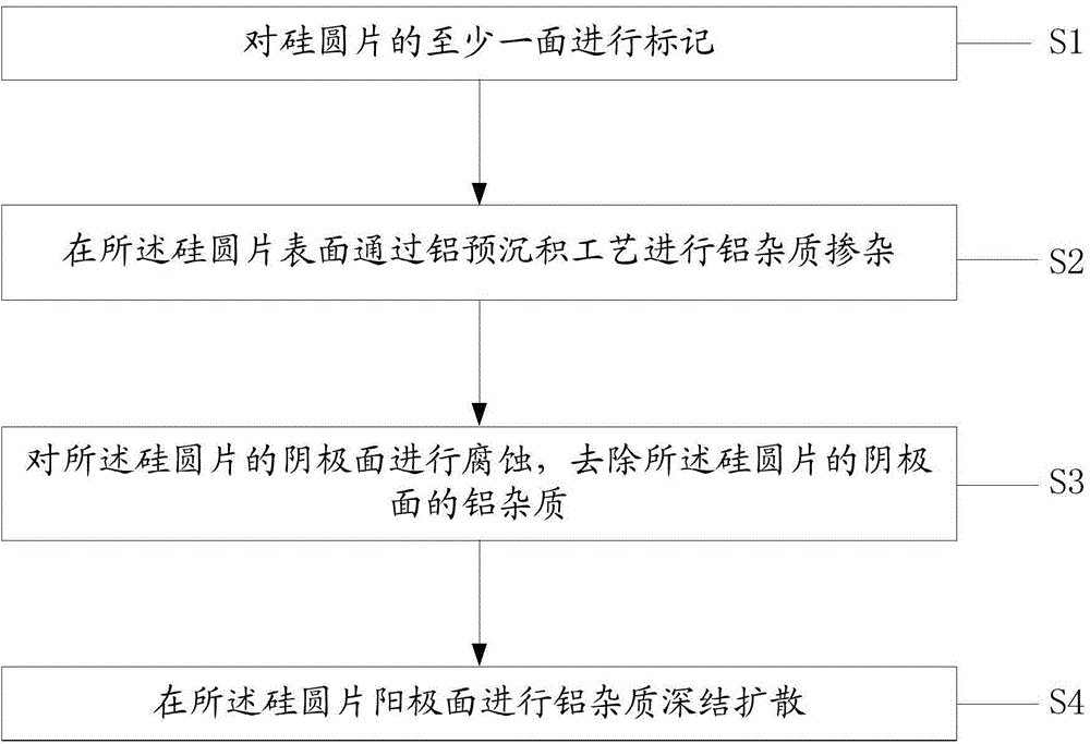
[0030] A method for manufacturing a high-power rectifier tube core provided by the embodiment of the present application is as follows: figure 1 as shown, figure 1 It is a schematic diagram of a manufacturing method of a high-power rectifier tube core provided by the embodiment of the present application. The method comprises the steps of:

[0031] S1: marking at least one side of the silicon wafer;

[0032] Since there is no single-side grinding step in th...


PUM


Abstract

The invention discloses a manufacturing method of a high-power rectification tube core. The method comprises the steps of marking at least one face of a silicon wafer; conducting aluminum impurity doping on the surface of the silicon wafer through the aluminum pre-deposition technology; corroding the cathode face of the silicon wafer, and removing aluminum impurities on the cathode face of the silicon wafer; conducting aluminum impurity deep-junction diffusion on the anode face of the silicon wafer. By means of the manufacturing method, surface defects and micro cracks of the silicon wafer can be prevented from being generated, and therefore the finished product rate and the long-term reliability of the high-power rectification tube core can be improved.

Description

technical field [0001] The invention relates to the technical field of chip manufacturing, in particular to a method for manufacturing a high-power rectifier tube core. Background technique [0002] Due to the extremely high current passing through the high-power device during operation, a very small amount of defects may cause device failure. Therefore, in the manufacturing process, the quality requirements for raw materials are very high. If there are many defects on the surface of the raw material, the leakage current of the device will be too large and the blocking voltage will be too low. Therefore, after the silicon single crystal rod is cut into silicon single crystal wafers, fine grinding must be performed, and chemical etching is also required after grinding to further remove defects on the grinding surface. The silicon single wafer grinding process has extremely strict requirements on the grinding equipment. It is necessary to ensure that there are no obvious defe...

Claims


Application Information

Patent Timeline
IPC IPC(8): H01L21/329
CPCH01L29/66083
Inventor 郭润庆邹冰艳颜骥王政英陈芳林唐革刘芹
Owner ZHUZHOU CRRC TIMES SEMICON CO LTD
Why Eureka
Try Eureka