Integrated method of surface channel CMOS (complementary metal oxide semiconductor) logic device and SONOS (silicon-oxide-nitride-oxide-silicon) device

A surface channel and logic device technology, which is applied in semiconductor/solid-state device manufacturing, electrical components, circuits, etc., can solve the problems of inability to realize the integration of surface channel CMOS logic devices and SONOS devices, the inability to resist polysilicon penetration, device leakage, etc. problems, to achieve the effect of realizing the integration of small-sized surface channel devices and high-density storage devices, reducing the size, and reducing the size

Active Publication Date: 2015-04-29
SHANGHAI HUAHONG GRACE SEMICON MFG CORP
View PDF5 Cites 4 Cited by
  • Summary
  • Abstract
  • Description
  • Claims
  • Application Information

AI Technical Summary

Problems solved by technology

When the device size is further reduced to 90 nanometers, or even 65 nanometers, the thickness of the gate oxide layer is further reduced, which cannot resist the boron in the polysilicon penetrating into the channel through the gate oxide layer, causing serious leakage of the device
[0006] As can be seen from the above, since the boron implantation of the polysilicon gate of the surface channel PMOS device in the existing

Method used


Image

  • Integrated method of surface channel CMOS (complementary metal oxide semiconductor) logic device and SONOS (silicon-oxide-nitride-oxide-silicon) device
  • Integrated method of surface channel CMOS (complementary metal oxide semiconductor) logic device and SONOS (silicon-oxide-nitride-oxide-silicon) device
  • Integrated method of surface channel CMOS (complementary metal oxide semiconductor) logic device and SONOS (silicon-oxide-nitride-oxide-silicon) device

Examples


Embodiment Construction

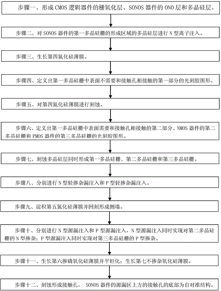
[0031] Such asfigure 1 Shown is the flow chart of the method of the embodiment of the present invention; Figure 2A to Figure 2J Shown is a device structure diagram in each step of the method of the embodiment of the present invention. The surface channel CMOS logic device in the integration method of the surface channel CMOS logic device and the SONOS device in the embodiment of the present invention includes a surface channel NMOS device and a surface channel PMOS device, including the following steps:

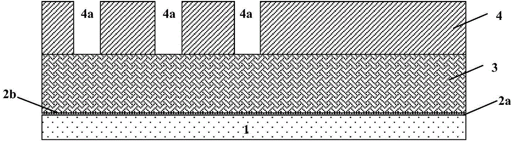
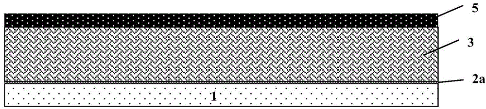
[0032] Step 1, such as Figure 2A As shown, the gate oxide layer 2a of the surface channel NMOS device and the surface channel PMOS device is formed on the surface of the silicon substrate 1 in the formation area of ​​the surface channel CMOS logic device, and in the formation area of ​​the SONOS device The ONO layer 2B of the SONOS device is formed on the surface of the silicon substrate 1, and the ONO layer 2B is composed of a first layer of silicon oxide, a second layer ...


PUM

PropertyMeasurementUnit
Thicknessaaaaaaaaaa
Thicknessaaaaaaaaaa
Thicknessaaaaaaaaaa

Abstract

The invention discloses an integrated method of a surface channel CMOS (complementary metal oxide semiconductor) logic device and an SONOS (silicon-oxide-nitride-oxide-silicon) device. The method comprises steps as follows: a gate oxide layer, an ONO layer and a polycrystalline silicon layer are formed; a gate polycrystalline silicon layer of the SONOS device is subjected to N type ion implantation; a fourth silicon nitride film is grown; a photoresist pattern of a first part of a first polysilicon gate is defined; the fourth silicon nitride film is etched; photoresist patterns of a second part of the first polysilicon gate and a polysilicon gate of the CMOS device are defined; polysilicon gates of the devices are formed while the polycrystalline silicon layer is etched; LDD (lightly doped drain) injection is performed; side walls are formed; source drain injection is performed; polysilicon gate doping of the CMOS logic device is realized while the source drain injection is performed; PSG (phosphosilicate glass) is grown and flattened; USG (undoped silicon glass) is grown; and contact holes are formed. With the adoption of the integrated method, a thermal process of boron penetration of a PMOS (P-channel metal oxide semiconductor) device can be reduced, the number of photoetching models is reduced, and a small-size surface channel device and a high-density storage device can be integrated.

Description

technical field [0001] The invention relates to a semiconductor integrated circuit manufacturing process method, in particular to an integration method of a surface channel CMOS logic device and a SONOS (silicon / silicon dioxide / silicon nitride / silicon dioxide / silicon) device. Background technique [0002] In the small-sized surface channel process, it is necessary to take into account the application of the high-end logic process, that is, the integration of the surface channel CMOS logic device process and the SONOS process. [0003] In surface channel CMOS logic devices, both NMOS devices and PMOS devices are surface channels. The surface channel requires the polysilicon gate of the NMOS device to be N-type doped, while the polysilicon gate of the PMOS device is P-type doped. Therefore, for surface channel CMOS logic devices, the doping of polysilicon gates of NMOS devices and PMOS devices should be carried out separately. Generally, the polysilicon gates of surface channe...

Claims


Application Information

Patent Timeline
IPC IPC(8): H01L21/77H01L21/8238
CPCH01L21/77H01L21/8238
Inventor 袁苑陈瑜陈华伦
Owner SHANGHAI HUAHONG GRACE SEMICON MFG CORP
Why Eureka
Try Eureka