Stress-released GaN-based LED structure and manufacturing method
A light-emitting diode and stress release technology, applied in electrical components, circuits, semiconductor devices, etc., can solve problems such as complex processes, and achieve the effects of improving wavelength uniformity, improving yield, and eliminating stress.
- Summary
- Abstract
- Description
- Claims
- Application Information
AI Technical Summary
Problems solved by technology
Method used
Image
Examples
no. 1 example
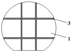
[0028] In the first embodiment, the GaN-based light-emitting diode structure provided by the present invention has a cross section as figure 1 shown, including SiO with bar 2 The sapphire substrate 1 and the GaN-based epitaxial layer 2 of the isolation zone 3, wherein the GaN-based epitaxial layer 2 includes a GaN buffer layer, an N-type GaN layer, a light emitting layer, and a P-type GaN material layer. The production method of this embodiment is as follows:
[0029] 1. Fabricate two rows and two columns of SiO on the growth surface of the sapphire substrate by PECVD 2 Strip barrier 3, such as figure 2 As shown, each SiO 2 The isolation zone 3 has a thickness of 15-20um and a width of 20um;
[0030] 2. A GaN-based epitaxial layer is grown by MOCVD on the growth surface of the sapphire substrate except the isolation zone.
no. 2 example
[0031] In the second embodiment, the GaN-based light-emitting diode structure provided by the present invention has a cross section as image 3 shown, including bars with Si x N y The sapphire substrate 1 and the GaN-based epitaxial layer 2 of the isolation zone 3, wherein the GaN-based epitaxial layer 2 includes a GaN buffer layer, an N-type GaN layer, a light emitting layer, and a P-type GaN material layer. The production method of this embodiment is as follows:
[0032] 1. Fabricate single-row and single-column Si on the growth surface of the sapphire substrate by PECVD x N y Strip barrier 3, such as Figure 4 As shown, each SiO 2 The isolation zone 3 has a thickness of 10-15um and a width of 20um;
[0033] 2. A GaN-based epitaxial layer is grown by MOCVD on the growth surface of the sapphire substrate except the isolation zone 3 .
no. 3 example
[0034] In the third embodiment, the GaN-based light-emitting diode structure provided by the present invention has a cross-section as Figure 5 As shown, it includes a sapphire substrate 1 with a strip-shaped isolation trench 4 and a GaN-based epitaxial layer 2, wherein the GaN-based epitaxial layer 2 includes a GaN buffer layer, an N-type GaN layer, a light-emitting layer, and a P-type nitride layer. Gallium material layer. The production method of this embodiment is as follows:
[0035] 1. Etch two rows and two columns of strip-shaped isolation trenches 4 on the sapphire substrate through the ICP process, such as Image 6 As shown, the depth of the isolation trench is 10-15um and the width is 20um;
[0036] 2. A GaN-based epitaxial layer is grown by MOCVD on the growth surface of the sapphire substrate except for the isolation trench.
[0037] In the specific examples listed above, the growth surface of the sapphire substrate has been subjected to growth isolation treatme...
PUM
| Property | Measurement | Unit |
|---|---|---|
| Width | aaaaa | aaaaa |
| Thickness | aaaaa | aaaaa |
| Width | aaaaa | aaaaa |
Abstract
Description
Claims
Application Information
 - R&D
- Intellectual Property
- Life Sciences
- Materials
- Tech Scout
- Unparalleled Data Quality
- Higher Quality Content
- 60% Fewer Hallucinations
Browse by: Latest US Patents, China's latest patents, Technical Efficacy Thesaurus, Application Domain, Technology Topic, Popular Technical Reports.
© 2025 PatSnap. All rights reserved.Legal|Privacy policy|Modern Slavery Act Transparency Statement|Sitemap|About US| Contact US: help@patsnap.com


