Manufacturing method and structure of low-temperature polycrystalline silicon TFT substrate

A technology of low-temperature polysilicon and its manufacturing method, which is applied in semiconductor/solid-state device manufacturing, electrical components, electric solid-state devices, etc., and can solve problems affecting the quality of low-temperature polysilicon TFT substrates, poor uniformity of the display area, and the electron mobility of the driving circuit in the driving area to be improved. and other issues, to achieve the effect of high quality, uniform electrical properties, and easy operation

Active Publication Date: 2015-05-06
SHENZHEN CHINA STAR OPTOELECTRONICS TECH CO LTD
View PDF4 Cites 12 Cited by
  • Summary
  • Abstract
  • Description
  • Claims
  • Application Information

AI Technical Summary

Problems solved by technology

[0015] However, the low-temperature polysilicon TFT substrate includes a display area and a driving area located in a non-display area. In the low-temperature polysilicon TFT substrate produced by the above method, the uniformity of the display area is poor, and the electron mobility of the driving circuit in the driving area is also to be determined. Improve, and then affect the quality of low-temperature polysilicon TFT substrate

Method used


Image

  • Manufacturing method and structure of low-temperature polycrystalline silicon TFT substrate
  • Manufacturing method and structure of low-temperature polycrystalline silicon TFT substrate
  • Manufacturing method and structure of low-temperature polycrystalline silicon TFT substrate

Examples


Embodiment Construction

[0055] In order to further illustrate the technical means adopted by the present invention and its effects, the following describes in detail in conjunction with preferred embodiments of the present invention and accompanying drawings.

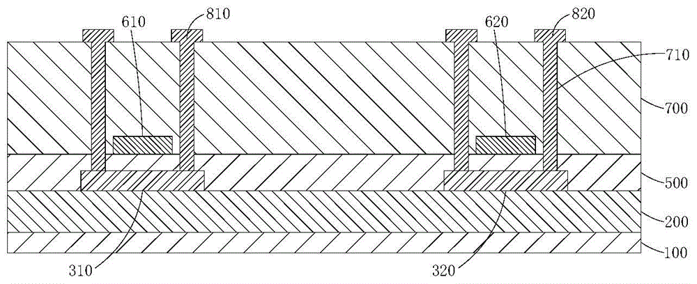
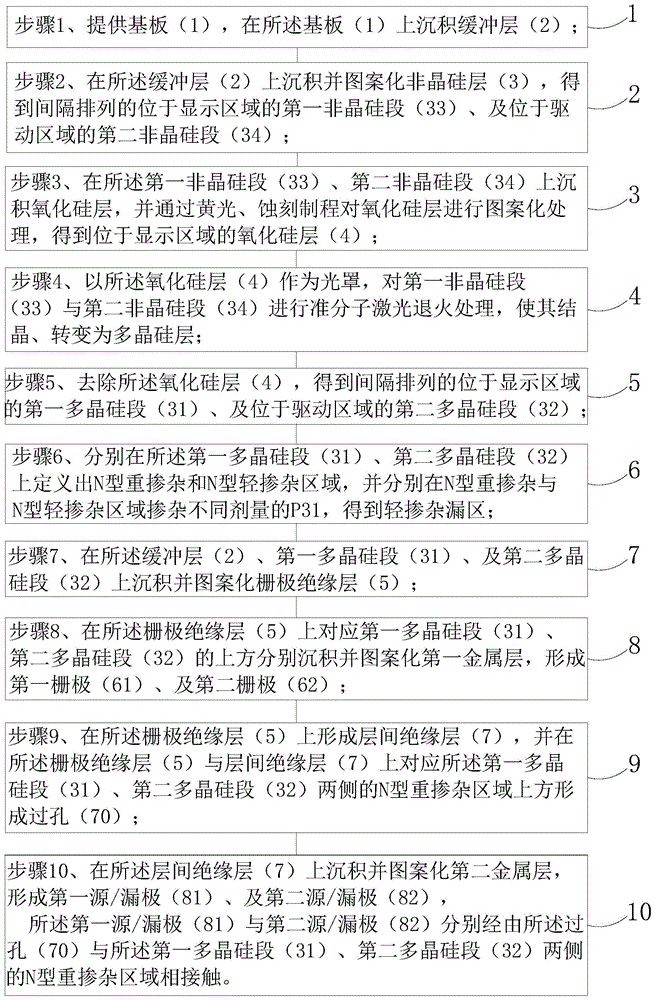
[0056] see figure 1 , the invention provides a method for manufacturing a low-temperature polysilicon TFT substrate, comprising the steps of:

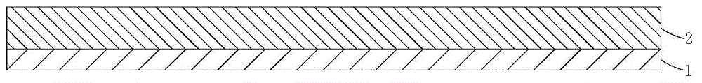
[0057] Step 1, such as image 3 As shown, a substrate 1 is provided on which a buffer layer 2 is deposited.

[0058] The substrate 1 is a transparent substrate, preferably, the substrate 1 is a glass substrate or a plastic substrate.

[0059] Specifically, the material of the buffer layer 2 may be silicon nitride (SiNx), silicon oxide (SiOx), or a combination of both.

[0060] Step 2, such as Figure 4-5 As shown, the amorphous silicon layer 3 is deposited and patterned on the buffer layer 2 to obtain first amorphous silicon segments 33 located in the display area and second amorphous silicon segme...


PUM


Abstract

The invention provides a manufacturing method and a structure of a low-temperature polycrystalline silicon TFT substrate. The method comprises the step 1 of providing a substrate (1) and depositing a buffer layer (2), the step 2 of depositing and patterning an amorphous silicon layer (3), the step 3 of depositing and patterning a silicon oxide layer (4), the step 4 of performing excimer laser annealing treatment on the amorphous silicon layer (3) with the silicon oxide layer (4) as a photomask so that the amorphous silicon layer (3) can be crystalized and converted into a polycrystalline silicon layer, the step 5 of obtaining a first polycrystalline silicon section (31) and a second polycrystalline silicon section (32), the step 6 of defining an N type heavy-doped region and an N type light-doped region on the first polycrystalline silicon section (31) and the second polycrystalline silicon section (32), respectively, and obtaining a light-doped drain region, the step 7 of depositing and patterning a gate insulation layer (5), the step 8 of forming a first gate (61) and a second gate (62), the step 9 of forming a via hole (70), and the step 10 of forming a first source/drain (81) and a second source/drain (82).

Description

technical field [0001] The invention relates to the field of display technology, in particular to a manufacturing method and structure of a low-temperature polysilicon TFT substrate. Background technique [0002] Thin-film transistor liquid crystal display (TFT-LCD) is divided into polysilicon (Poly-Si) technology and amorphous silicon (a-Si) technology, low temperature polysilicon (Low Temperature Poly-silicon, LTPS) technology is The biggest difference between the manufacturing technology of the new generation of thin film transistor liquid crystal display and the traditional amorphous silicon display is that the low temperature polysilicon display has a faster response speed, and has the advantages of high brightness, high resolution and low power consumption. [0003] The silicon crystal arrangement of low-temperature polysilicon is more orderly than that of amorphous silicon, so that the electron mobility is relatively higher by more than 100 times. The peripheral drivi...

Claims


Application Information

Patent Timeline
Patent Type & Authority Applications(China)
IPC IPC(8): H01L21/77H01L27/12
CPCH01L21/77H01L27/12H01L27/1214
Inventor 卢改平
Owner SHENZHEN CHINA STAR OPTOELECTRONICS TECH CO LTD
Why Eureka
Try Eureka