Measuring method for intermediate-state energy level of energy gap of semiconductor material

A measurement method, semiconductor technology, applied in the field of nanosecond time-resolved spectroscopic measurement, can solve the problem of not being able to provide information on the positions of the initial state and the final state of the bound state, cannot detect delocalized electrons, and cannot be used to determine the bound state and conduction Band transition energy level and other issues

Inactive Publication Date: 2015-05-13
INST OF PHYSICS - CHINESE ACAD OF SCI
View PDF0 Cites 9 Cited by
  • Summary
  • Abstract
  • Description
  • Claims
  • Application Information

AI Technical Summary

Problems solved by technology

[0003] Electron paramagnetic resonance (EPR) can characterize the bound electrons in titanium dioxide (Ti 3+ ) and bound holes (O - ,O 2 - ), but the EPR technique cannot detect delocalized electrons in the conduction band, so it cannot be used to determine the bound state and the transition energy level of the conduction band; spectroscopy has been widely used to detect conduction band electrons, bound state electrons, hole and transition energy levels, but current spectroscopic experimental methods cannot provide information on the positions of the initial and final states with respect to the bound states, but only determine the energy difference between the initial and final states

Method used


Image

  • Measuring method for intermediate-state energy level of energy gap of semiconductor material
  • Measuring method for intermediate-state energy level of energy gap of semiconductor material
  • Measuring method for intermediate-state energy level of energy gap of semiconductor material

Examples


no. 1 example

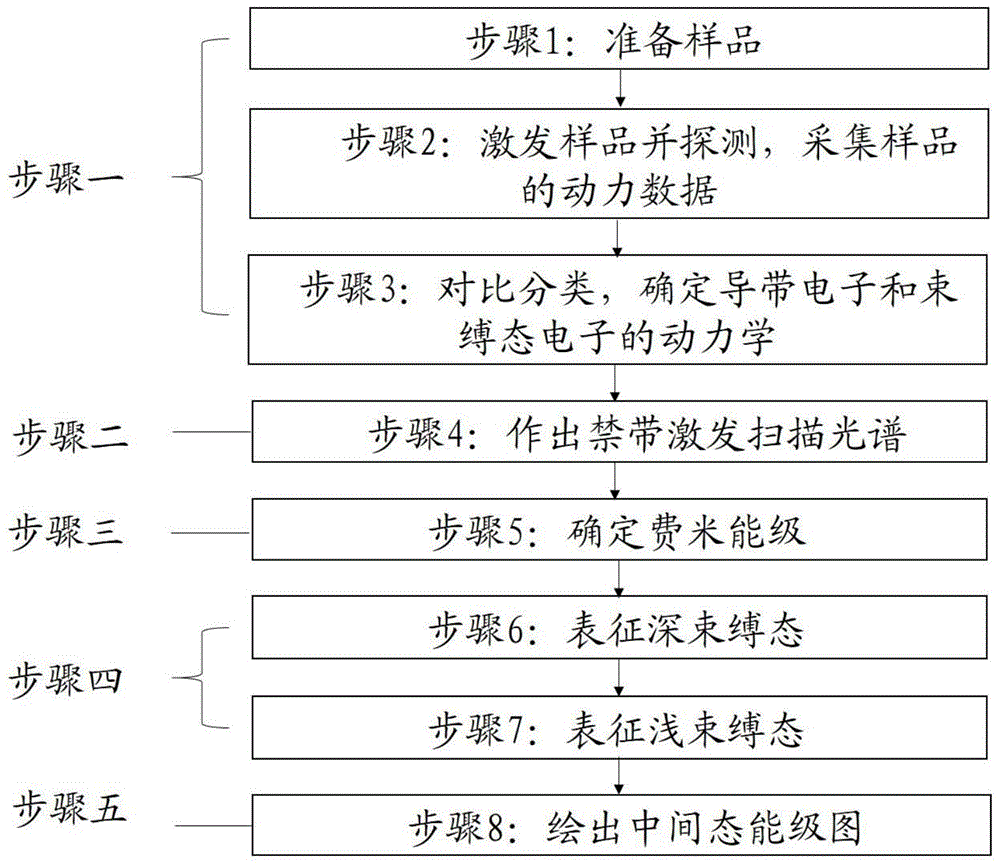
[0047] According to the first embodiment of the present invention, measuring anatase TiO 2 The steps of the energy gap intermediate state energy level of semiconductor material are as follows:

[0048] Step 1: Anatase TiO coated on a 1-inch calcium fluoride substrate 2 The thin film is placed in the sample cell, in which, the anatase TiO 2 The average particle size of nanoparticles is 8nm;

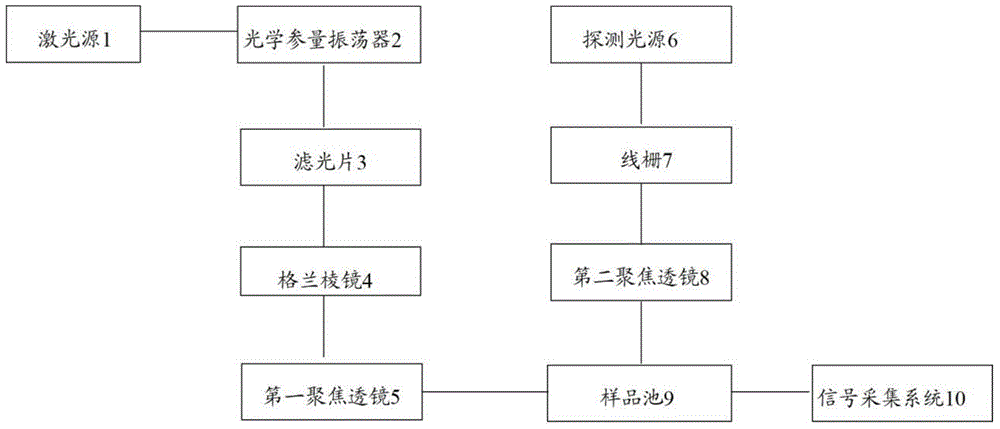
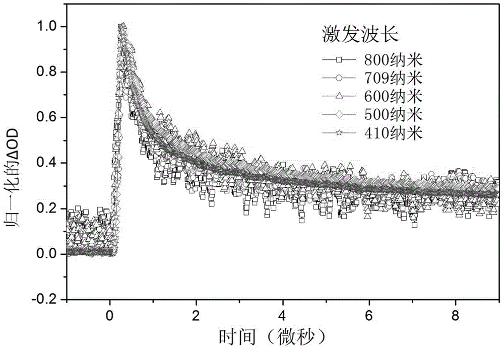
[0049] Step 2: Adopt figure 1 In the device shown, multiple excitation lights with different wavelengths in the range of 410-1500nm are sequentially selected to excite the sample. For 410nm-650nm, the wavelength is selected with a step of 5nm; for 710nm-1500nm, the wavelength is selected with a step of 10nm, and the excitation The light energy is 0.5mJ / pulse, and the wavelength is 4.78μm (2090cm -1 ) detection light to detect the photogenerated carriers in the excited sample; display the dynamic process of the carrier after the sample is excited by the excitation light of different wavel...

no. 2 example

[0066] In the second embodiment, a wavelength of 6.25 μm (1600 cm -1 ) of the detection light detects the photogenerated carriers in the excited sample, and obtains the transient infrared absorption kinetics and anatase TiO in the same way as the first embodiment 2 Bandgap Excitation Scan Spectra. Figure 8 The detection wavelength is 6.25μm (1600cm -1 ) of anatase TiO 2 bandgap excitation scan spectrum, which is related to Figure 5 Probe wavelength shown is 4.78μm (2090cm -1 ) of anatase TiO 2 The shape of the bandgap excitation scan spectrum is very similar. Repeat steps 5-step 8 of the first embodiment on this basis, also obtain Figure 7 The anatase TiO shown 2 Distribution of all intermediate state energy levels in the forbidden band.

no. 3 example

[0068] In addition to anatase TiO 2 , another important TiO 2 rutile TiO 2 . In the third embodiment, the measurement of rutile TiO 2 The intermediate state energy level of the energy gap, the steps are as follows:

[0069] Step 1: rutile TiO with an average particle size of 100nm 2 The nano film is placed in the sample cell;

[0070] Step 2: Adopt figure 2 In the device shown, multiple excitation lights with different wavelengths in the range of 410-1500nm are sequentially selected to excite the sample. For 410nm-650nm, the wavelength is selected with a step of 5nm; for 710nm-1500nm, the wavelength is selected with a step of 10nm, and the excitation The light energy is 5.0mJ / pulse, and the wavelength is 4.78μm (2090cm -1 ) detection light to detect the photogenerated carriers in the excited sample; display the dynamic process of the carrier after the sample is excited by the excitation light of different wavelengths through the oscilloscope, and collect the kinetics a...


PUM

PropertyMeasurementUnit
particle sizeaaaaaaaaaa

Abstract

The invention provides a measuring method for intermediate-state energy level of an energy gap of a semiconductor material. The measuring method comprises the following steps: step I: acquiring dynamic data, under different excitation wavelengths, of the semiconductor material, and distinguishing dynamics of conduction band electrons from dynamics of bound state electrons; step II: mapping according to value, at the same time, of the dynamic data after pulse excitation, thereby obtaining a forbidden band excitation scanning spectrum of the semiconductor material; step III: determining fermi energy level of the semiconductor material; step IV: according to the fermi energy level and the forbidden band excitation scanning spectrum, representing a bound state of the semiconductor material; step V: drawing a band gap intermediate-state energy level diagram of the semiconductor material. According to the measuring method, the position of fermi energy level can be determined and the intermediate-state energy level of the semiconductor material can be symmetrically represented, so that the design of photocatalysts is guided to develop towards practicability and high efficiency.

Description

technical field [0001] The invention belongs to the technical field of nanosecond time-resolved spectral measurement, and in particular relates to a method for measuring the energy level of an intermediate state in the energy gap of a semiconductor material. Background technique [0002] Titanium dioxide is considered to be one of the best materials for photocatalysis and solar energy conversion. However, due to the wide band gap of titanium dioxide, titanium dioxide absorbs only in the range of ultraviolet rays, accounting for 3-5% of the total sunlight, and the light conversion efficiency in the solar spectrum region is very low. Therefore, extending the TiO2 absorption to the visible range is an effective means to improve the light conversion efficiency. The introduction of defect states in titanium dioxide can not only reduce the probability of electron-hole recombination, but also change the width of the energy gap, so that titanium dioxide has high activity in the sol...

Claims


Application Information

Patent Timeline
Patent Type & Authority Applications(China)
IPC IPC(8): G01N21/63G01N21/3563
Inventor 翁羽翔米阳
Owner INST OF PHYSICS - CHINESE ACAD OF SCI
Why Eureka
Try Eureka