Preparation method of GaN-based LED epitaxial structure

An epitaxial structure, N-type technology, applied in electrical components, circuits, semiconductor devices, etc., can solve the problems of low luminous efficiency and uneven electron distribution of GaN-based light-emitting epitaxial structures, and achieve enhanced internal quantum efficiency, uniform distribution, and improved Effect of Luminous Efficiency

Inactive Publication Date: 2015-05-13
ENRAYTEK OPTOELECTRONICS
View PDF7 Cites 16 Cited by
  • Summary
  • Abstract
  • Description
  • Claims
  • Application Information

AI Technical Summary

Problems solved by technology

[0006] In view of the shortcomings of the prior art described above, the purpose of the present invention is to provide a method for preparing a GaN-based LED epitaxial structure, which is used to solve the problems cause

Method used


Image

  • Preparation method of GaN-based LED epitaxial structure
  • Preparation method of GaN-based LED epitaxial structure
  • Preparation method of GaN-based LED epitaxial structure

Examples


Embodiment 1

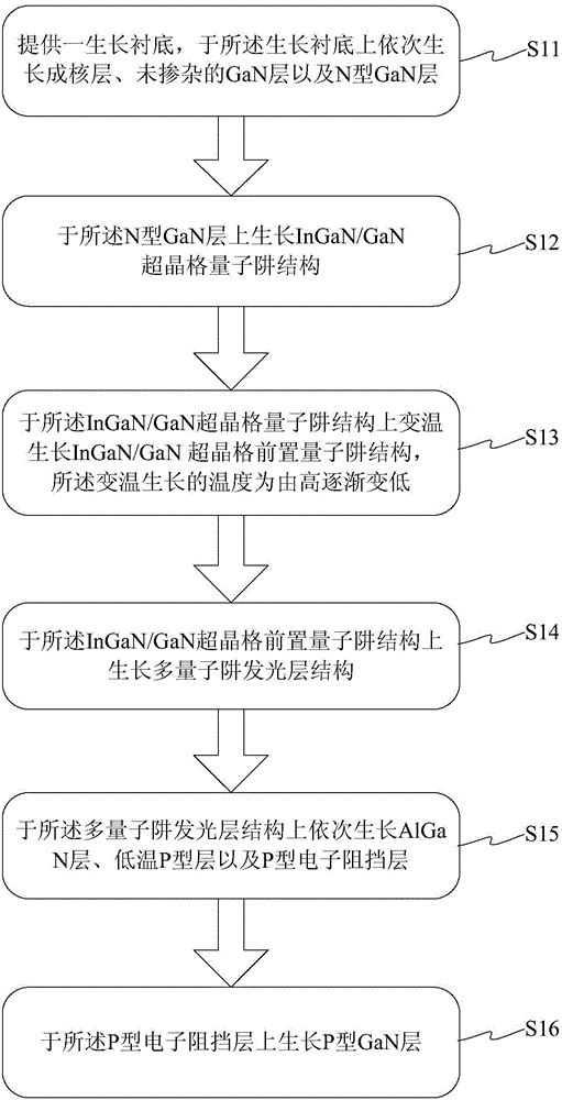
[0056] Such as Figure 1 to Figure 7 As shown, this embodiment provides a method for preparing a GaN-based LED epitaxial structure, and the preparation method includes steps:

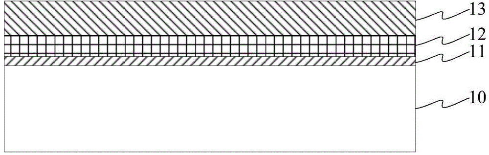
[0057] Such as figure 1 and figure 2 As shown, step 1) S11 is first performed to provide a growth substrate 10 on which a nucleation layer 11 , an undoped GaN layer 12 and an N-type GaN layer 13 are sequentially grown.

[0058] As an example, the growth substrate 10 may be sapphire, GaN, silicon, silicon carbide, etc. In this embodiment, the growth substrate 10 is a sapphire substrate.

[0059] Specifically, this step includes the following sub-steps:

[0060] In step 1-1), a sapphire substrate is provided, and a nucleation layer 11 is grown on the surface of the sapphire substrate at a temperature of 450-650° C., and the growth thickness of the nucleation layer 11 is in the range of 15-50 nm.

[0061] Step 1-2), growing an undoped GaN layer 12 on the surface of the nucleation layer 11 at a tempera...

Embodiment 2

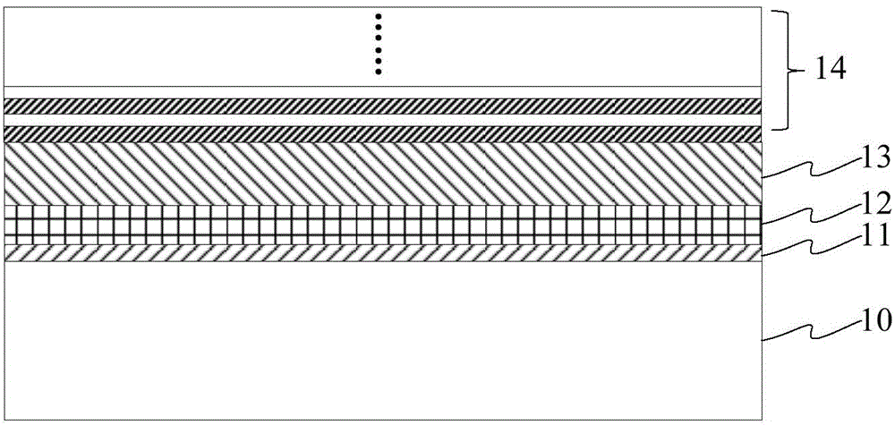
[0087] Such as Figure 7 As shown, this embodiment provides a GaN-based LED epitaxial structure, and the GaN-based LED epitaxial structure includes a nucleation layer 11, an undoped GaN layer 12, an N-type GaN layer 13, and an InGaN / GaN supercrystalline layer stacked in sequence. Lattice quantum well structure 14, InGaN / GaN pre-quantum well structure 15 grown gradually from high temperature to low temperature, multi-quantum well light-emitting layer structure 16, AlGaN layer 17, low-temperature P-type layer 18, P-type electron blocking layer 19, and P-type GaN layer 20 .

[0088] Such as Figure 7 As shown, the GaN-based LED epitaxial structure is formed on a growth substrate 10 including one of sapphire, GaN, silicon and silicon carbide. In this embodiment, the GaN-based LED epitaxial structure is formed on a sapphire substrate.

[0089] The thickness range of the nucleation layer 11 is 15-50nm; the total thickness range of the undoped GaN layer 12 and the N-type GaN layer...


PUM

PropertyMeasurementUnit
Growth temperatureaaaaaaaaaa
Thicknessaaaaaaaaaa
Thicknessaaaaaaaaaa

Abstract

The invention discloses a preparation method of a GaN-based LED epitaxial structure. The preparation method comprises the following steps of: preparing a nucleating layer, an undoped GaN layer, an N-type GaN layer, and an InGaN/GaN superlattice quantum well structure all which are sequentially laminated; growing an InGaN/GaN preposed quantum well structure, a multi-quantum-well light-emitting layer structure, an AlGaN layer, a low-temperature P-type layer, a P-type electron blocking layer and a P-type GaN layer by gradually changing the temperature from high temperature to low temperature. The preparation method is characterized in that the InGaN/GaN preposed quantum well structure is grown by a temperature-changing method, electron distribution in the light-emitting quantum well can be modulated by the preposed quantum well structure according to the flowing method of buffered electrons to the P end, so that the electrons can be uniformly distributed in the light-emitting quantum well, the internal quantum efficiency is enhanced and the light-emitting efficiency of the epitaxial structure is improved.

Description

technical field [0001] The invention belongs to the field of semiconductor lighting, in particular to a method for preparing a GaN-based LED epitaxial structure. Background technique [0002] Light Emitting Diode (LED, Light Emitting Diode) has been widely used in various fields due to its advantages of long life and low energy consumption, especially as its lighting performance index is greatly improved day by day, LED is often used as a light emitting device in the lighting field. Among them, the III-V compound semiconductor represented by gallium nitride (GaN), especially the InGaN / GaN (indium gallium nitride / gallium nitride)-based LED has a wide band gap, high luminous efficiency, and electron saturation drift speed. High, stable chemical properties, etc., have great application potential in the field of high-brightness blue light-emitting diodes, blue lasers and other optoelectronic devices, and have attracted widespread attention. [0003] However, due to the large la...

Claims


Application Information

Patent Timeline
IPC IPC(8): H01L33/00H01L33/06H01L33/14
CPCH01L33/0075H01L33/06H01L33/14
Inventor 琚晶马后永李起鸣
Owner ENRAYTEK OPTOELECTRONICS
Why Eureka
Try Eureka