Isolated NLDMOS (N type Laterally Diffused Metal Oxide Semiconductor) device

An isolation type and device technology, which is applied in semiconductor devices, semiconductor/solid-state device manufacturing, electrical components, etc., can solve problems such as low breakdown voltage and unbalanced size change, and achieve the goal of improving breakdown voltage and current drive capability Effect

Active Publication Date: 2015-05-20
SHANGHAI HUAHONG GRACE SEMICON MFG CORP
View PDF4 Cites 2 Cited by
  • Summary
  • Abstract
  • Description
  • Claims
  • Application Information

AI Technical Summary

Problems solved by technology

From the comparison of the cross-sectional diagrams of tangent line A and tangent line B, it can be seen that the transition region between the cell region and the terminal drifts in the s

Method used


Image

  • Isolated NLDMOS (N type Laterally Diffused Metal Oxide Semiconductor) device
  • Isolated NLDMOS (N type Laterally Diffused Metal Oxide Semiconductor) device
  • Isolated NLDMOS (N type Laterally Diffused Metal Oxide Semiconductor) device

Examples


Embodiment 1

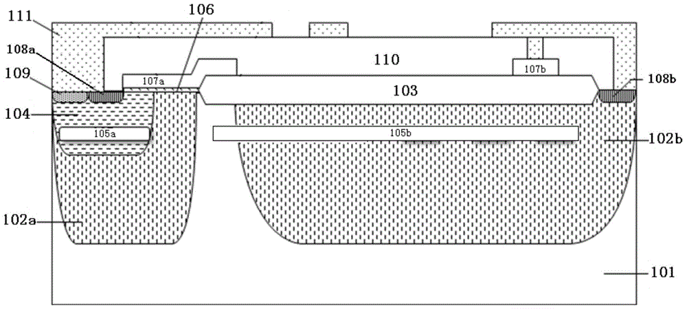
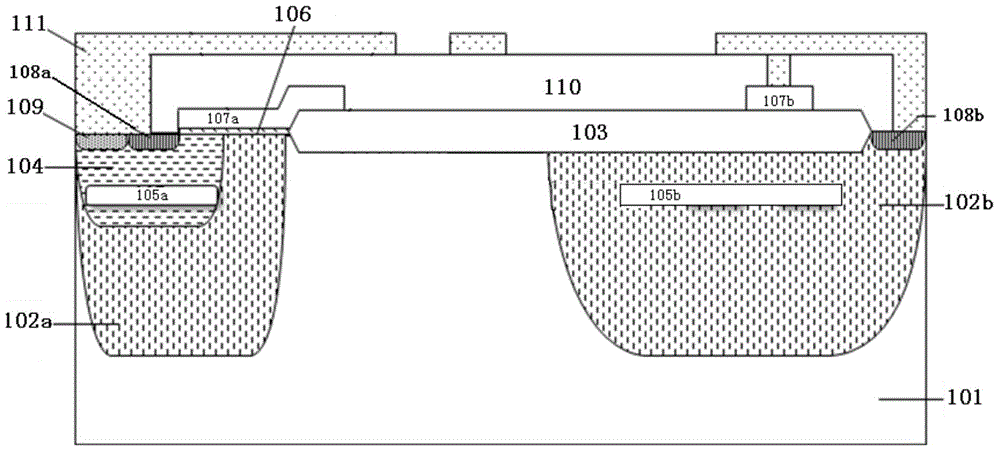
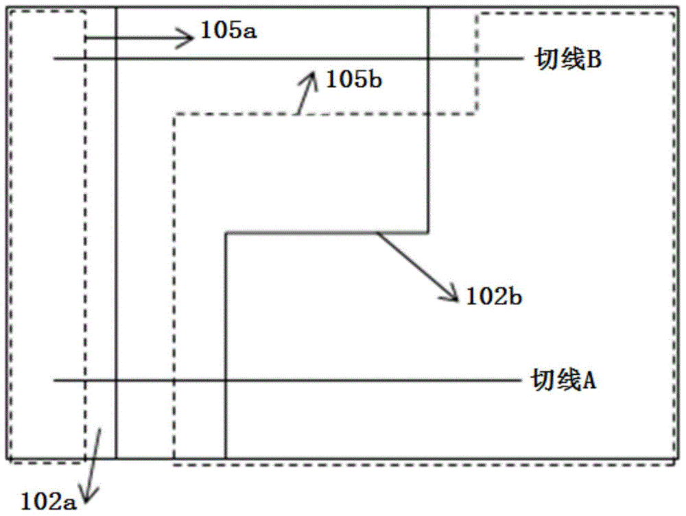
[0037] For isolated NLDMOS devices, the terminals are located at the upper and lower ends of the cell region, and the longitudinal cross-sectional structure of the cell region is as follows: figure 1 As shown, two independent N-type deep wells, a left N-type deep well 102a and a right N-type deep well 102b, are formed on the P-type silicon substrate 101;

[0038] The left N-type deep well 102a has a P well 104 formed on the left;

[0039] In the P well 104, a P-type heavily doped region 109 and a source N-type heavily doped region 108a are formed on the left;

[0040] A gate oxide layer 106 is formed above the right part of the P well 104 and above the right part of the left N-type deep well 102a;

[0041] Field oxygen 103 is formed above the P-type silicon substrate 101 between the left N-type deep well 102a and the right N-type deep well 102b, and above the left part of the right N-type deep well 102b;

[0042] The right N-type deep well 102b has a drain N-type heavily dop...

Embodiment 2

[0053] Based on the isolated NLDMOS device of Embodiment 1, a drain terminal polysilicon field plate 107b is formed above the right part of the field oxide 103;

[0054] The interlayer dielectric 110 covers the surface of the device;

[0055] The P-type heavily doped region 109 and the source N-type heavily doped region 108a are short-circuited together by a metal 111 passing through the interlayer dielectric 110;

[0056] The drain terminal N-type heavily doped region 108b is short-circuited with the drain terminal polysilicon field plate 107b through another metal 111 passing through the interlayer dielectric 110;

[0057] Preferably, a source end P-type implantation region 105a is formed in the P well 104 .


PUM


Abstract

The invention discloses an isolated NLDMOS (N type Laterally Diffused Metal Oxide Semiconductor) device. Terminals are positioned at the upper end and lower end of a cellular area; two independent N type deep traps are formed on a type P silicon substrate; field oxide is formed above the P type silicon substrate between a left N type deep trap and a right N type deep trap, and above the left part of the right N type trap; a drift P type injection area is formed in the P type silicon substrate and the right N type deep trap below the field oxide; the left N type deep trap, the right N type deep trap, the field oxide and the drift P type injection area extend toward an upper end and a lower end to the terminals; in the terminals, the left side of the right N type deep trap moves rightwards, the left side of the drift P type injection area moves rightwards, and the drift P type injection area is integrally arranged inside the right N type deep trap; in transition areas between the cellular area and the terminals, the left side of the right N type deep trap is in slowly changing transition; the left side of the drift P type injection area is slowly changing transition. By adopting the isolated NLDMOS device, the current driving capability can be enhanced, and the breakdown voltage is increased.

Description

technical field [0001] The invention relates to semiconductor technology, in particular to an isolated NLDMOS device. Background technique [0002] LDMOS (Laterally Diffused Metal Oxide Semiconductor) is currently widely used in power management circuits due to its advantages of high voltage resistance, high current drive capability, extremely low power consumption, and integration with CMOS. [0003] The isolated NLDMOS device not only has the high-voltage and high-current characteristics of discrete devices, but also absorbs the advantages of high-density intelligent logic control of low-voltage integrated circuits. A single chip realizes the functions that can only be completed by multiple chips, which greatly reduces the area, reduces costs, and improves It meets the development direction of miniaturization, intelligence and low energy consumption of modern power electronic devices. Breakdown voltage and on-resistance are key parameters for measuring isolated NLDMOS dev...

Claims


Application Information

Patent Timeline
IPC IPC(8): H01L29/78H01L29/06H01L21/336H01L21/265
CPCH01L29/66681H01L29/7816H01L29/7835
Inventor 段文婷刘冬华钱文生
Owner SHANGHAI HUAHONG GRACE SEMICON MFG CORP
Why Eureka
Try Eureka