MEMS (micro-electro mechanical system) pressure sensor and forming method thereof

A pressure sensor and pressure technology, which is applied in the measurement of fluid pressure, piezoelectric devices/electrostrictive devices, and fluid pressure measurement through electromagnetic components, etc. question

Active Publication Date: 2015-05-27
MEMSEN ELECTRONICS
View PDF6 Cites 13 Cited by
  • Summary
  • Abstract
  • Description
  • Claims
  • Application Information

AI Technical Summary

Problems solved by technology

[0007] In the existing manufacturing methods of MEMS pressure sensors, the process of integrating the pressure sensor chip and the signal processing circuit is quite different, and it is difficult to achieve monolithic integration.
At the same time, when the integrated circuit and the pressure sensor are fabricated on a single substrate, the existence of the pressure sensor has hindered the development of the integrated circuit, and the existence of the integrated circuit on the same substrate has also caused difficulties in the manufacture of small-sized pressure sensors.
Therefore, the manufacturing process of using a single substrate as an integrated circuit and a pressure sensor is more complicated

Method used


Image

  • MEMS (micro-electro mechanical system) pressure sensor and forming method thereof
  • MEMS (micro-electro mechanical system) pressure sensor and forming method thereof
  • MEMS (micro-electro mechanical system) pressure sensor and forming method thereof

Examples


Embodiment 1

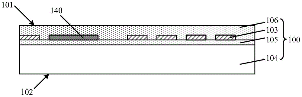
[0103] Figure 1 to Figure 9 It is a schematic cross-sectional structure diagram of the forming process of the MEMS pressure sensor of the embodiment of the present invention.

[0104] Please refer to figure 1 , providing a first substrate 100, the first substrate 100 includes an opposite first surface 101 and a second surface 102, the first substrate 100 includes at least one conductive layer 103, and the conductive layer 103 is located at the The side of the first surface 101 of the first substrate 100 described above.

[0105] In this embodiment, the first substrate 100 also has a fixed electrode 140, and the fixed electrode 140 is located on the side of the first surface 101 of the first substrate 100; After the first surface 101 and the third surface of the second substrate are fixed to each other, the fixed electrode 140 is arranged opposite to the pressure-sensitive electrode, and a cavity is formed between the pressure-sensitive electrode and the fixed electrode, so ...

Embodiment 2

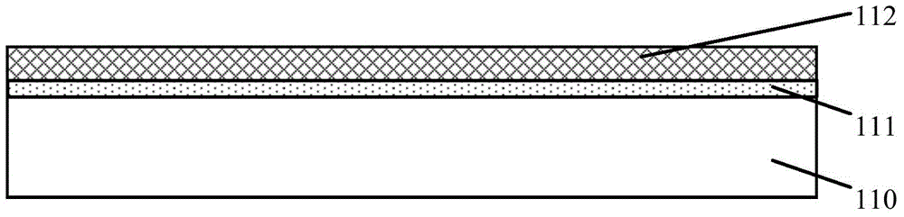
[0185] Figure 10 to Figure 11 It is a schematic cross-sectional structure diagram of the formation process of the MEMS pressure sensor according to another embodiment of the present invention.

[0186] Please refer to Figure 10 , a first substrate 200 is provided, the first substrate 200 includes an opposite first surface 201 and a second surface 202, the first substrate 200 includes at least one conductive layer 203, and the conductive layer 203 is located on the On the side of the first surface 201 of the first substrate 200 , the first substrate 200 further includes a self-test electrode 230 .

[0187] The first substrate 200 further includes a fixed electrode 240, and the fixed electrode 240 is located on the side of the first surface 201 of the first substrate 200; After the third surfaces of the substrates are fixed to each other, the fixed electrodes 240 correspond to the pressure-sensitive electrodes, and a cavity needs to be formed between the pressure-sensitive e...

Embodiment 3

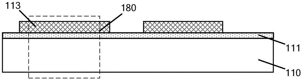
[0204] Figure 12 to Figure 15 It is a schematic cross-sectional structure diagram of the forming process of the MEMS pressure sensor according to another embodiment of the present invention.

[0205] Please refer to Figure 12 , providing a second substrate 314, the second substrate 314 includes an opposing third surface 318 and a fourth surface 319, the second substrate 314 includes a second base 310 and a pressure-sensitive pressure sensor on the second base 310 An electrode 313, the second substrate 314 includes a pressure sensing region 380, the pressure sensitive electrode 313 is located in the pressure sensing region 380, the pressure sensitive electrode 313 is located on the third side of the second substrate 314 On the surface 318 side, the second substrate 314 further includes a reference cell region 331 .

[0206] The pressure-sensitive electrode 313 is also formed in the reference cell region 331 .

[0207] In this embodiment, the second substrate 314 further in...


PUM


Abstract

The invention discloses an MEMS (micro-electro mechanical system) pressure sensor and a forming method thereof. The forming method comprises steps as follows: a first substrate comprising a first surface and a second surface is provided and comprises at least one conductive layer which is located on one side of the first surface of the first substrate; a second substrate comprising a third surface and a fourth surface is provided and comprises a second base, a pressure-sensitive electrode and a pressure sensing area, and the pressure-sensitive electrode is located in the pressure sensing area and is located on one side of the third surface of the second substrate; the first surface of the first substrate is fixed with the third surface of the second substrate, and a hollow cavity is formed between the first substrate and the pressure sensing area of the second substrate; the second base is removed, and a fifth surface opposite to the third surface of the second substrate is formed; a first conductive plug penetrating to the at least one conductive layer is formed on one side of the fifth surface of the second substrate, so that the at least one conductive layer and the pressure-sensitive electrode are electrically connected. According to the MEMS pressure sensor and the forming method thereof, the performance and the reliability of the MEMS pressure sensor are improved, the size is reduced, and the processing cost is reduced.

Description

technical field [0001] The invention relates to the technical field of semiconductor manufacturing, in particular to a MEMS pressure sensor and a forming method thereof. Background technique [0002] Micro-Electro Mechanical System (MEMS for short) is an integrated device that acquires information, processes information and performs operations. Sensors in MEMS can receive external information such as pressure, position, velocity, acceleration, magnetic field, temperature or humidity, and convert the obtained external information into electrical signals for processing in MEMS. Common microelectromechanical systems include temperature sensors, pressure sensors, and humidity sensors. [0003] For the MEMS pressure sensor, its size is smaller, and its process precision, and its manufacturing process can be compatible with the manufacturing process of integrated circuit chips, thus greatly improving the cost performance. Current MEMS pressure sensors include piezoresistive pres...

Claims


Application Information

Patent Timeline
IPC IPC(8): G01L1/14G01L9/12G01L23/12B81B3/00B81C1/00
CPCG01L9/0042G01L9/0073
Inventor 周文卿
Owner MEMSEN ELECTRONICS
Why Eureka
Try Eureka