Plasma-enhanced chemical vapor deposition preparation method of multi-layered graphene film

A multi-layer graphene, plasma technology, applied in gaseous chemical plating, coating, metal material coating process and other directions, can solve problems such as process constraints, high cost, etc., achieve simple and easy-to-control preparation conditions and processes, raw materials Widely sourced and inexpensive effects

Inactive Publication Date: 2015-06-03
ZHEJIANG HANNAO DIGITAL TECH
View PDF3 Cites 7 Cited by
  • Summary
  • Abstract
  • Description
  • Claims
  • Application Information

AI Technical Summary

Problems solved by technology

High-quality large-area graphene can be prepared by chemical vapor deposition, which meets the requirements for large-scale preparation of high-quality graphene, but at this stage, high cost, complicated process and precise control of processing conditions restrict chemical vapor deposition. The development of the preparation of graphene, so the method still needs further research

Method used


Image

  • Plasma-enhanced chemical vapor deposition preparation method of multi-layered graphene film
  • Plasma-enhanced chemical vapor deposition preparation method of multi-layered graphene film

Examples


preparation example Construction

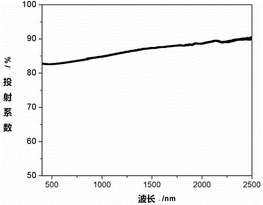
[0018] The preparation of step 2 multilayer graphene film: the amorphous SiC nano film on the quartz or glass substrate obtained in step 1 is used as a buffer layer, and the plasma-enhanced chemical vapor deposition preparation method is used to directly deposit multiple layers on the buffer layer For the graphene film, the deposition temperature is controlled at 450-950 degrees Celsius. The obtained multi-layer graphene film has a uniform thickness and a high visible light transmittance of 60-90%.

[0019] The radio frequency magnetron sputtering method uses 99.999% high-purity argon gas, the sputtering power is controlled at about 50 watts, and the time is controlled at about 30 seconds.

[0020] The described plasma-enhanced chemical vapor deposition preparation method adopts CH 4 and H 2 As a gas source, CH4:H2 in the gas source is 1.5:1, the power is controlled at about 150 watts, the temperature of the quartz or glass substrate is controlled at about 500 degrees ...

Embodiment 1

[0023] (1) Deposit SiC nano-film on quartz or glass substrate: use 99.9% SiC ceramic target, background vacuum 3 mPa, sputtering gas 99.999% high-purity argon, sputtering power 50 watts, time 30 Seconds, the temperature of the glass substrate is 400 degrees Celsius. The resulting amorphous film had a thickness of 3 nm.

[0024] (2) Preparation of multilayer graphene film: use the glass sheet prepared in step (1) as the substrate, use CH4 and H2 composite gas as the gas source, and the ratio of the composite gas in the gas source is CH4:H2=1.5:1 , the power is 150 watts, the substrate temperature is 500 degrees Celsius, the time is 10 minutes, and the obtained film thickness is 5 nm.

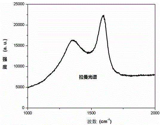
[0025] The optical transmittance of the multilayer graphene film that present embodiment makes is as follows figure 1 As shown, the raman spectrum is as figure 2 shown. From figure 1 It can be seen that the visible light transmittance of the film is greater than 80%, while figure 2 Th...


PUM

PropertyMeasurementUnit
Thicknessaaaaaaaaaa

Abstract

The invention relates to a plasma-enhanced chemical vapor deposition preparation method of a multi-layered graphene film. The method comprises the following steps: depositing a SiC nano-film on a quartz or glass substrate; plating a layer of amorphous SiC nano-film with the thickness of 2-5 nm on the quartz or glass substrate by using a SiC ceramic as a sputtering target material by adopting a radio frequency magnetron sputtering method, wherein the temperature of the quartz or glass substrate is controlled to be at 400-500 DEG C; directly depositing the multi-layered graphene film on a buffer layer which is the amorphous SiC nano-film prepared in the step in on the quartz or glass substrate by using the plasma-enhanced chemical vapor deposition preparation method to obtain the multi-layered graphene film, wherein the temperature is controlled to be at 450-950 DEG C. The obtained multi-layered graphene film is uniform in thickness and relatively high in visible light transmittance.

Description

technical field [0001] The invention relates to a plasma-enhanced chemical vapor deposition preparation method of a multilayer graphene film, which belongs to the field of inorganic nanometer materials. Background technique [0002] The preparation of graphene mainly includes physical methods and chemical methods. Physical methods usually use cheap graphite or expanded graphite as raw materials to prepare monolayer or multilayer graphene by micromechanical exfoliation method, liquid phase or gas phase direct exfoliation method. Alkenes have high purity and fewer defects, but are time-consuming and low-yield, making them unsuitable for large-scale production. At present, graphene used in laboratories is mainly prepared by chemical methods, mainly focusing on chemical vapor deposition methods. The chemical vapor deposition method of graphene usually heats the substrate with catalytic function to 1000°C in the cavity, and then passes through carbon-containing gas, such as...

Claims


Application Information

Patent Timeline
IPC IPC(8): C23C16/44C23C16/26C23C16/02
CPCC23C16/26C23C16/0272C23C16/44
Inventor 郭正
Owner ZHEJIANG HANNAO DIGITAL TECH
Why Eureka
Try Eureka