Forming method of CMOS (complementary metal-oxide-semiconductor) transistor

A technology of transistors and semiconductors, applied in semiconductor devices, semiconductor/solid-state device manufacturing, electrical components, etc., can solve the problems of mask layer material residue, difficult to remove, and affect the quality of gates, etc., to achieve improved aspect ratio and easy The effect of removal

Inactive Publication Date: 2015-06-03
SEMICON MFG INT (SHANGHAI) CORP
View PDF5 Cites 1 Cited by
  • Summary
  • Abstract
  • Description
  • Claims
  • Application Information

AI Technical Summary

Problems solved by technology

However, organic materials are difficult to remove, so when the mask layer is subsequently removed, there will be mask layer material residues, which will affect the quality of the gate formed in the subsequent process and affect the performance of the CMOS transistor.
[0005] Therefore, the performance of the CMOS transistors formed by the prior art needs to be further improved.

Method used


Image

  • Forming method of CMOS (complementary metal-oxide-semiconductor) transistor
  • Forming method of CMOS (complementary metal-oxide-semiconductor) transistor
  • Forming method of CMOS (complementary metal-oxide-semiconductor) transistor

Examples


Embodiment Construction

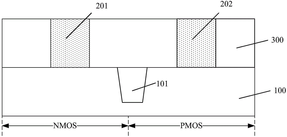
[0031] As mentioned in the background art, the performance of the CMOS transistors formed in the prior art needs to be further improved.

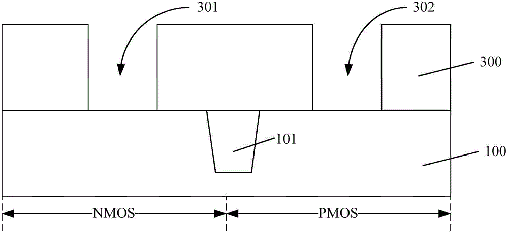
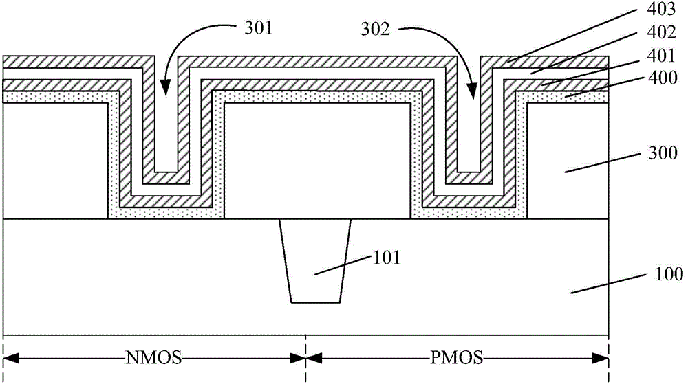
[0032] In the prior art, in the process of forming the NMOS transistor and the PMOS transistor, the same work function layer is formed in the NMOS region and the PMOS region at the same time, and then after the mask layer is formed in the PMOS region, the PMOS work function layer on the NMOS region is removed, so that Subsequent formed CMOS transistors and PMOS transistors have different work functions. The material of the mask layer is an organic material such as a photoresist layer or a bottom anti-reflection material. Although the filling effect of the mask layer in the groove for forming the grid can be improved, the organic material is removed during the removal process. Easy to leave residue. In the prior art, a mask layer is usually formed on the NMOS and PMOS regions at the same time, and then the mask layer on the NMOS region is r...


PUM


Abstract

The invention provides a forming method of a CMOS (complementary metal-oxide-semiconductor) transistor. The forming method comprises the following steps that a semiconductor substrate is provided, and the semiconductor substrate comprises an NMOS (N-channel metal oxide semiconductor) region, a PMOS (P-channel metal oxide semiconductor) region, a first groove positioned in the surface of the NMOS region and a second groove positioned in the surface of the PMOS region; a grid dielectric material layer, a first metal layer, a second metal layer and a third metal layer are sequentially formed on the surfaces of the inner walls of the first groove and the second groove and the surface of a dielectric layer; covering material layers filling into the first groove and the second groove are formed, the materials of the covering material layers are insulation dielectric materials; the covering material layer on the NMOS region is removed; the covering material layer at partial thickness in the second groove is removed for forming a covering layer; a third metal layer and a second metal layer in the first groove, above the dielectric layer as well as above the covering layer and in the second groove are removed; the covering layer is removed; a first grid electrode and a second grid electrode are formed in the first groove and the second groove. The forming method of the CMOS transistor has the advantage that the performance of the CMOS transistor can be improved.

Description

technical field [0001] The invention relates to the technical field of semiconductors, in particular to a method for forming a CMOS transistor. Background technique [0002] With the continuous improvement of the integration level of semiconductor devices and the reduction of technology nodes, the traditional gate dielectric layer continues to become thinner, and the leakage of transistors increases accordingly, causing problems such as waste of power consumption of semiconductor devices. In order to solve the above problems, the prior art provides a solution of replacing the polysilicon gate with a metal gate. Among them, the "gate last" process is a main process for forming high-K metal gate transistors. [0003] The existing method for forming a high-K metal gate transistor using a gate-last process includes: providing a semiconductor substrate on which a dummy gate structure is formed and located on the semiconductor substrate and covering the dummy gate structure The ...

Claims


Application Information

Patent Timeline
Patent Type & Authority Applications(China)
IPC IPC(8): H01L21/8238H01L21/28
CPCH01L21/8238H01L29/4236H01L29/66477
Inventor 三重野文健
Owner SEMICON MFG INT (SHANGHAI) CORP
Why Eureka
Try Eureka