Supercharge Your Innovation With Domain-Expert AI Agents!

Device for on-line real-time detection of epitaxial film growth

A technology for real-time detection and epitaxial wafers, which is applied in semiconductor/solid-state device testing/measurement, material excitation analysis, Raman scattering, etc. It can solve the problems of small molecular Raman scattering cross-section, difficulty in coordination, and huge amount of real-time detection data. , to achieve the effect of simple structure and reducing poor quality

Active Publication Date: 2015-06-10
北京艾瑞豪泰信息技术有限公司
View PDF6 Cites 1 Cited by
  • Summary
  • Abstract
  • Description
  • Claims
  • Application Information

AI Technical Summary

Problems solved by technology

[0003] However, the technical difficulties encountered in the measurement of on-line photoluminescence spectroscopy include: (1) The molecular Raman scattering cross section is small, and the excitation and collection of Raman signals are difficult; (2) For real-time detection systems, the acquisition speed of the spectrometer, Parameters such as pulse laser frequency and MOCVD reaction speed are not easy to coordinate; (3) The amount of real-time detection data is huge. Taking the speed of 1200rpm as an example, the amount of detection data per second can reach 20M. Therefore, the online The photoluminescence spectroscopy measurement device has high requirements on the hardware

Method used


Image

  • Device for on-line real-time detection of epitaxial film growth
  • Device for on-line real-time detection of epitaxial film growth
  • Device for on-line real-time detection of epitaxial film growth

Examples


Embodiment 1

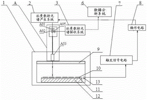
[0054] See attached figure 2 , the on-line detection device for epitaxial film growth used to produce semiconductor quantum devices provided by Embodiment 1 of the present invention. Including MOCVD reaction chamber 1, Raman scattering spectrum generation system 2, Raman scattering spectrum receiving system 3, working signal circuit 4, signal conversion circuit 5, data analysis system 6', trigger signal circuit 7 and operation circuit 8, the signal The conversion circuit 5 has both the A / D signal conversion function and the D / A signal conversion function.

[0055] The MOCVD reaction chamber is followed by a heater 12, a graphite disk 11, and an epitaxial wafer 10 from bottom to top. The upper part of the MOCVD reaction chamber 1 is sealed by quartz glass 9, and the MOCVD reaction chamber 1 is in a vacuum environment. Figure 6 , is a schematic structural diagram of the arrangement of the epitaxial wafers 10 on the graphite disk 11 . See attached Figure 5 , There is a slit...


PUM


Abstract

The invention discloses a device for on-line real-time detection of epitaxial film growth, and belongs to the technical field of semiconductor material manufacturing equipment. The device comprises an MOCVD reaction chamber, an optical component, a Raman scattering spectroscopy production system, a Raman scattering spectra of receiving system, a data analysis system, a photoelectric switch, a trigger signal circuit and an operating circuit. The device has the advantages of simple structure, easy coordination of parameters and obviously reduced real-time detection data bulk.

Description

technical field [0001] The invention relates to the technical field of semiconductor material manufacturing equipment, in particular to a device for on-line real-time detection of epitaxial wafer growth. Background technique [0002] Scattering occurs when light hits a substance. When scattering occurs, the wavelength of a small part of the scattered light will increase or decrease, that is, Raman scattering occurs, and the spectrum corresponding to Raman scattering is called Raman spectrum. Raman spectroscopy belongs to the vibrational spectrum of molecules. Each substance has its own characteristic Raman spectrum, so Raman spectrum can usually be used as a "fingerprint" for identifying substances, in which the Raman spectra of different materials have their own spectrum-characteristic spectrum that is different from other materials . The elements of the reaction are the driving substances provided in the equipment. Different temperatures and different contents can be us...

Claims


Application Information

Patent Timeline
Patent Type & Authority Applications(China)
IPC IPC(8): G01N21/65H01L21/66
Inventor 李成敏严冬叶龙茂王林梓刘健鹏刘涛
Owner 北京艾瑞豪泰信息技术有限公司
Features
  • R&D
  • Intellectual Property
  • Life Sciences
  • Materials
  • Tech Scout
  • Unparalleled Data Quality
  • Higher Quality Content
  • 60% Fewer Hallucinations
Learn More