Technological method for manufacturing groove type Schottky diodes

A technology of Schottky diode and preparation process, which is applied in semiconductor/solid-state device manufacturing, electrical components, circuits, etc., can solve the problems of small process window, low product yield, large reverse leakage current, etc., to improve product yield efficiency, low reverse leakage, and the effect of reducing reverse leakage

Active Publication Date: 2015-06-10
SHANGHAI HUAHONG GRACE SEMICON MFG CORP
View PDF5 Cites 8 Cited by
  • Summary
  • Abstract
  • Description
  • Claims
  • Application Information

AI Technical Summary

Problems solved by technology

At present, the commonly used preparation method is to etch the contact hole by dry method, and then directly deposit the metal to form the Sc

Method used


Image

  • Technological method for manufacturing groove type Schottky diodes
  • Technological method for manufacturing groove type Schottky diodes
  • Technological method for manufacturing groove type Schottky diodes

Examples


Embodiment Construction

[0024] The present invention will be described in further detail below in conjunction with the accompanying drawings and embodiments.

[0025] Such as Figure 1-Figure 6 Shown, the preparation technology method of trench Schottky diode of the present invention comprises the following steps:

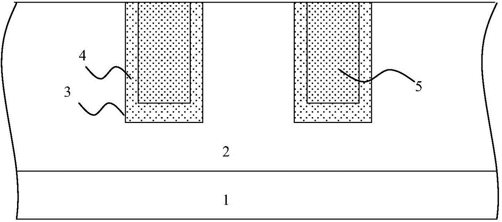
[0026] 1. If figure 1 Shown: Referring to the standard trench-type Schottky diode manufacturing process, an epitaxial layer 2 is grown on a silicon substrate 1 (the epitaxial layer 2 has the same doping type as the silicon substrate 1), and the epitaxial layer 2 is etched to form Trench 3, deposit a layer of silicon oxide 4 in the trench 3, then fill the trench 3 with polysilicon, and then use dry etching to etch back the polysilicon outside the trench 3, and retain the polysilicon in the trench 5.

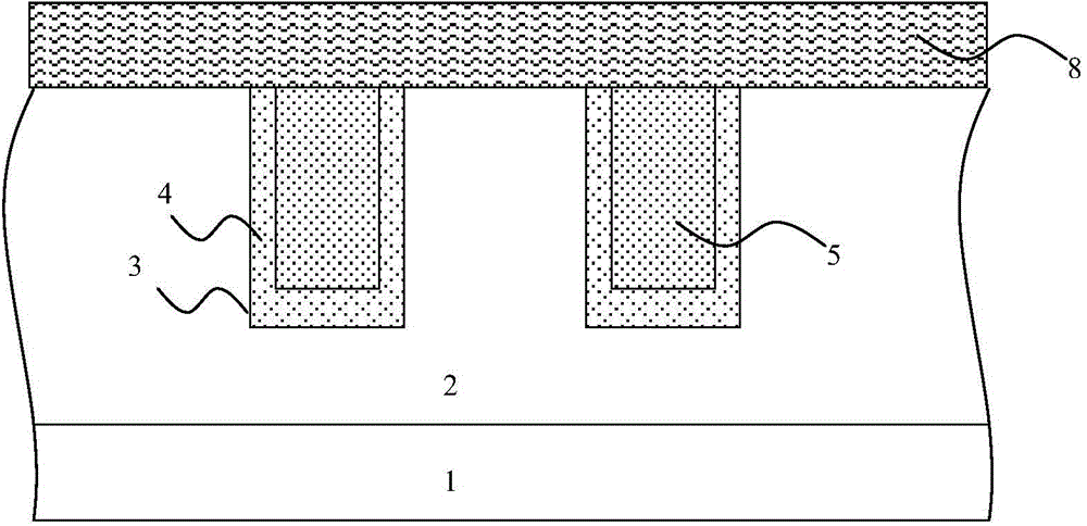
[0027] 2. If figure 2 As shown: a layer of oxide is deposited on the silicon surface as an interlayer dielectric film 8 by using a CVD (chemical vapor deposition) process. The interlayer...


PUM

PropertyMeasurementUnit
Thicknessaaaaaaaaaa

Abstract

The invention discloses a technological method for manufacturing groove type Schottky diodes. Contact holes are particularly formed by means of etching by the aid of two-step dry processes. The technological method includes etching silicon surfaces at first when the contact holes are about to be formed; then etching silicon and silicon oxide in grooves together. Selection ratios of the silicon to the silicon oxide in last-step contact hole etching menus are 1:1, the silicon surfaces are etched by depths higher than 1000 angstroms approximately, the silicon oxide in the side walls of the grooves is protruded out of the silicon surfaces, and Schottky contact effects are ultimately realized by the aid of metal. The technological method has the advantages that the technological method aims to solve the problem of high electric leakage of existing groove Schottky diode products, the internal uniformity of the surfaces of products can be improved, the production cost can be reduced, the yield of the products can be increased, and the technological method is suitable for mass production on a large scale.

Description

technical field [0001] The invention relates to a manufacturing process of a semiconductor integrated circuit, in particular to a manufacturing process method of a trench Schottky diode. Background technique [0002] Schottky diodes are well known in the industry and are fabricated through a variety of different layout designs and processes. The trench-type layout typically shown in Baliga's US Patent No. 5,612,567 is also known. The trench-type Schottky diode pursues the maximization of the forward conduction current capability, and its mesa area is fully utilized in Schottky. The base barrier contacts, which requires the contact hole to fully open the cell area during etching. At present, the commonly used preparation method is to dry-etch the contact hole, and then directly deposit metal to form the Schottky contact, but the actual process will cause problems such as small process window, large reverse leakage current, and low product yield. Contents of the invention ...

Claims


Application Information

Patent Timeline
IPC IPC(8): H01L21/329H01L29/06H01L29/872
CPCH01L29/0603H01L29/0684H01L29/872H01L29/8725
Inventor 李昊刘远良
Owner SHANGHAI HUAHONG GRACE SEMICON MFG CORP
Why Eureka
Try Eureka