Radiofrequency LDMOS (laterally diffused metal oxide semiconductor) device and manufacturing method thereof

A device and radio frequency technology, which is applied in the field of semiconductor integrated circuit manufacturing, can solve the problems of increased concentration in the drift region 103 and prone to hot carrier effects, etc.

Active Publication Date: 2015-06-10
SHANGHAI HUAHONG GRACE SEMICON MFG CORP
View PDF5 Cites 2 Cited by
  • Summary
  • Abstract
  • Description
  • Claims
  • Application Information

AI Technical Summary

Problems solved by technology

However, it is difficult to increase the concentration of the drift region 103 of the RF LDMOS device to a very high level by relying on G-shield a

Method used


Image

  • Radiofrequency LDMOS (laterally diffused metal oxide semiconductor) device and manufacturing method thereof
  • Radiofrequency LDMOS (laterally diffused metal oxide semiconductor) device and manufacturing method thereof
  • Radiofrequency LDMOS (laterally diffused metal oxide semiconductor) device and manufacturing method thereof

Examples


Embodiment Construction

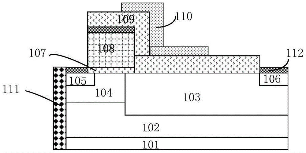
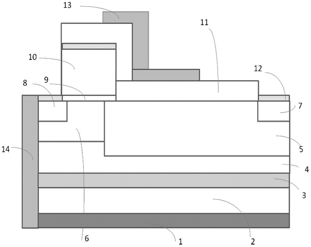
[0065] Such as figure 2 As shown, it is a schematic structural diagram of the radio frequency LDMOS device of the embodiment of the present invention; the radio frequency LDMOS device of the embodiment of the present invention includes:

[0066] A heavily doped silicon substrate 1 of the first conductivity type. Preferably, the doping concentration of the silicon substrate 1 is greater than 1e20cm -3 .

[0067] A silicon epitaxial layer doped with the first conductivity type, the silicon epitaxial layer is formed by stacking a first silicon epitaxial layer 2, a second silicon epitaxial layer 3 and a third silicon epitaxial layer 4 sequentially formed on the surface of the silicon substrate 1 become.

[0068] The drift region 5 is composed of a second conductivity type ion implantation region formed in a selected region of the third silicon epitaxial layer 4, the top surface of the drift region 5 and the top surface of the third silicon epitaxial layer 4 In other words, th...


PUM

PropertyMeasurementUnit
Thicknessaaaaaaaaaa

Abstract

The invention discloses a radiofrequency LDMOS (laterally diffused metal oxide semiconductor) device. A first silicon epitaxial layer, a second silicon epitaxial layer and a third silicon epitaxial layer are stacked in order on the bottom surface of a silicon substrate, forming a silicon epitaxial layer. A drift area and a trench area are both formed in the third silicon epitaxial layer. The second silicon epitaxial layer is formed at the bottoms of the drift area and the trench area. The doping density of the second silicon epitaxial layer is greater than that of the first and third silicon epitaxial layers. On resistance of the device and breakdown voltage of a drain junction are adjusted by adjusting the doping density of the third silicon epitaxial layer. The second silicon epitaxial layer is integrally provided with an inner RESURF structure (reduced surface field) structure, used for decreasing surface field of the drift area, thermal carrier effect and improving reliability of the radiofrequency LDMOS. The first silicon epitaxial layer helps maintain or increase the breakdown voltage of the drain junction. The device has the advantages that source-drain stray capacitance of the device can be improved, source-drain on resistance can be reduced, drive current can be increased and radiofrequency characteristic of the device can be improved.

Description

technical field [0001] The invention relates to the field of semiconductor integrated circuit manufacturing, in particular to a radio frequency LDMOS device; the invention also relates to a method for manufacturing the radio frequency LDMOS device. Background technique [0002] RF Lateral Field Effect Transistor (RF LDMOS) is a common device used in RF base stations and broadcasting stations. High breakdown voltage, low source-drain on-resistance (RDSON) and low source-drain parasitic capacitance (Coss) are device characteristics that RF LDMOS must have. Such as figure 1 Shown is a schematic structural diagram of an existing radio frequency LDMOS device. Taking an N-type device as an example, the existing radio frequency LDMOS device includes: a P-type heavily doped, ie P+ doped, silicon substrate 101, and the doping concentration of the silicon substrate 101 is Greater than 1e20cm -3 ; P-type lightly doped silicon epitaxial layer 102, the doping concentration and thickne...

Claims


Application Information

Patent Timeline
IPC IPC(8): H01L29/78H01L29/06H01L21/336
CPCH01L29/0611H01L29/063H01L29/66681H01L29/7816
Inventor 钱文生
Owner SHANGHAI HUAHONG GRACE SEMICON MFG CORP
Why Eureka
Try Eureka