

Method for manufacturing electron source
A manufacturing method and electron source technology, which are applied in the manufacture of discharge tubes/lamps, electrode systems, cold cathodes, etc., can solve problems such as the increase of energy amplitude and color difference, the stability of discharge current, and the inability to cope with it.
- Summary
- Abstract
- Description
- Claims
- Application Information
AI Technical Summary
Problems solved by technology
Method used
Image

Examples
Embodiment 1
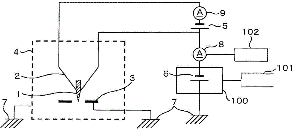
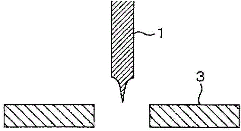
[0039] figure 2 A conceptual diagram showing an apparatus for processing substrates. The substrate 1 whose front end is sharpened by electrolytic grinding of tungsten single crystal filaments whose axis orientation is orientation is fixed in the heating element 2 and arranged in the vacuum container 4 . The heating element 2 is connected with a voltage source 6 for applying a voltage to the substrate 1, an ammeter 8 for measuring the amount of current discharged from the substrate 1, and a current source 5 for heating the heating element. In addition, a lead-out electrode 3 at ground potential is disposed near the substrate 1 , and an electric field is generated between the substrate 1 and the lead-out electrode 3 by applying a voltage to the heating element 2 . image 3 Represents details around the substrate.
[0040] The vacuum vessel 4 is vacuum exhausted from the 10 -4 Pa up to 10 -2 At a pressure of about Pa, the main component of the residual gas is water. In thi...
Embodiment 2
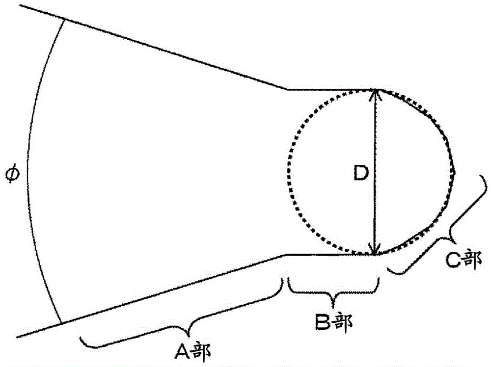
[0056] The so-called electrolytic polishing is a method of immersing a filament in an electrolytic solution and applying a voltage to grind the filament to produce a sharpened tip. However, at this time, the shape of the tip under the applied voltage of DC voltage and AC voltage is Different (hereinafter, the grinding based on DC voltage will be called DC electrolytic grinding, and the grinding based on AC voltage will be called AC electrolytic grinding). For tungsten single crystal filaments whose axis orientation is orientation, when direct current electrolytic polishing is performed, the angle (cone angle) of the conical portion at the tip of the substrate changes by alternating current electrolytic polishing. Figure 12 express its difference. When the front end is sharpened by DC electric field polishing, the front end of the substrate is ground into a curved shape, and the cone angle α becomes 10 degrees or less. When the substrate is sharpened by the method shown in E...
Embodiment 3
[0061] In the method of Example 1, the processing time of the substrate is arbitrarily determined, but it is possible to control the tip diameter by making the applied voltage constant and using the processing time as a parameter. When the voltage applied to the facility is 5kV and 3kV, the processing of the substrate starts immediately after the voltage is applied and ends every measured time (processing time), Figure 14 Represents a graph depicting the size of the diameter of the front end of the substrate. The horizontal axis represents machining time, and the vertical axis represents tip diameter. The diameter of the front end increases with a logarithmic function as the processing time increases, and gradually saturates. This saturated state is a state in which the front end diameter of the substrate is fixed to a certain thickness, and the larger the applied voltage, the larger the front end diameter becomes. Processing time to control the front diameter.
PUM
| Property | Measurement | Unit |
|---|---|---|
| diameter | aaaaa | aaaaa |
Abstract
Description
Claims
Application Information