Fringe-field switching mode thin film transistor array substrate and manufacturing method thereof

A thin-film transistor and fringe field switching technology, which is applied in the manufacture of semiconductor/solid-state devices, electric solid-state devices, semiconductor devices, etc., can solve the problems of rapid release of ionic impurities, residual ionic impurities, and residual ions, etc. Achieve the effect of enhancing fringe electric field, improving afterimage problem and reducing power consumption

Active Publication Date: 2015-06-17
KUSN INFOVISION OPTOELECTRONICS
View PDF4 Cites 13 Cited by
  • Summary
  • Abstract
  • Description
  • Claims
  • Application Information

AI Technical Summary

Problems solved by technology

When there is a DC bias, the ionic impurities remaining on the alignment layer are mixed into the liquid crystal molecules because they cannot be released in time, forming ion residues and causing afterimages
That is to say, due to the existence of DC bias, the ionic impurities accumulated in the liquid crystal molecules cannot be quickly released through the alignment layer, which may easily cause the ionic impurities to remain in the liquid crystal molecules, resulting in afterimage problems

Method used


Image

  • Fringe-field switching mode thin film transistor array substrate and manufacturing method thereof
  • Fringe-field switching mode thin film transistor array substrate and manufacturing method thereof
  • Fringe-field switching mode thin film transistor array substrate and manufacturing method thereof

Examples


Embodiment Construction

[0029] Embodiments of the present invention provide a fringe field switching mode thin film transistor array substrate and a manufacturing method thereof, which are beneficial to enhancing the fringe electric field, reducing the driving voltage of liquid crystal molecules, thereby reducing power consumption, and effectively improving afterimage problems during display. Each will be described in detail below.

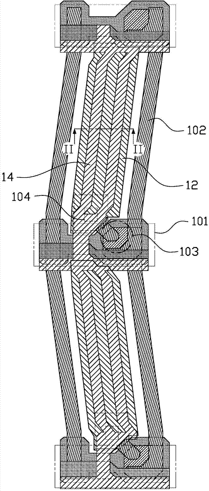
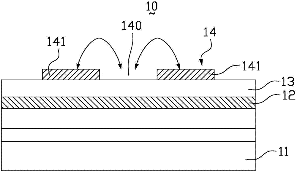
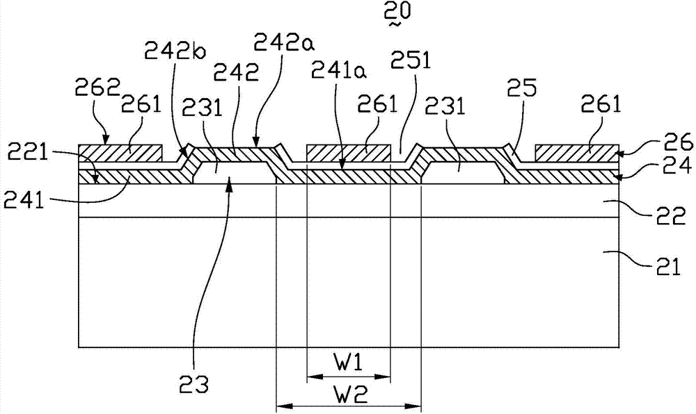
[0030] image 3 is a partial cross-sectional schematic diagram of a thin film transistor array substrate in fringe field switching mode according to the first embodiment of the present invention, please refer to image 3 The thin film transistor array substrate 20 in fringe field switching mode provided in the first embodiment includes a transparent substrate 21 and a plurality of scanning lines 101 formed on the transparent substrate 21 ( figure 1 ) and multiple data lines 102 ( figure 1), a plurality of scanning lines 101 and a plurality of data lines 102 intersect t...


PUM


Abstract

The invention discloses a fringe-field switching mode thin film transistor array substrate and a manufacturing method thereof. The array substrate comprises a first insulating layer formed on a transparent substrate, a second insulating layer formed on the first insulating layer, a first electrode layer formed on the second insulating layer, a third insulating layer formed on the first electrode layer and a second electrode layer formed on the third insulating layer, wherein the second insulating layer comprises multiple insulating protrusive portions arranged at intervals; the multiple insulating protrusive portions protrude out of the surface of the first insulating layer; the first electrode layer comprises multiple electrode flat portions and multiple electrode convex portions; the multiple electrode flat portions cover the surface, not provided with the insulating protrusive portions, of the first insulating layer; the multiple electrode convex portions cover the multiple insulating protrusion portions respectively; the upper surfaces of the electrode convex portions are not covered with the third insulating layer and exposed; the second electrode layer comprises multiple electrode portions arranged at intervals; the multiple electrode portions are located above the multiple electrode flat portions respectively; the electrode portions and the electrode convex portions are arranged in a staggered and alternate mode.

Description

technical field [0001] The invention relates to the field of display technology, in particular to a fringe field switching mode thin film transistor array substrate and a manufacturing method thereof. Background technique [0002] Liquid Crystal Display (LCD) has the advantages of good picture quality, small size, light weight, low driving voltage, low power consumption, no radiation and relatively low manufacturing cost, and it occupies a dominant position in the field of flat panel display. With the development of technology, people's demand for liquid crystal displays with high transmittance, high contrast, wide viewing angle and low power consumption continues to increase. The traditional twisted nematic mode (Twisted Nematic, TN) liquid crystal display panel has the problem of narrow viewing angle. In order to realize liquid crystal display with a wide viewing angle, the liquid crystal display panel of the in-plane switching mode (In-Plane Switching, IPS) using the tran...

Claims


Application Information

Patent Timeline
Patent Type & Authority Applications(China)
IPC IPC(8): G02F1/1343G02F1/1362G02F1/1368H01L27/12H01L23/485H01L21/84H01L21/48
CPCG02F1/134309G02F1/13452G02F1/136227G02F1/136286G02F1/1368H01L27/124H01L27/1259
Inventor 李东朝王俊李海波祝秀芬唐先柱
Owner KUSN INFOVISION OPTOELECTRONICS
Why Eureka
Try Eureka