Double-gate and double-pole graphene field effect transistor and manufacturing method thereof

A field effect transistor and a manufacturing method technology, applied in the field of double gate bipolar graphene field effect transistor and its manufacture, can solve the problems of impurity pollution, reduce G-FET performance, graphene defects, etc., and achieve economical cost and excellent development. off performance, the effect of small gate leakage current

Active Publication Date: 2015-06-17
SHANGHAI INST OF MICROSYSTEM & INFORMATION TECH CHINESE ACAD OF SCI
View PDF3 Cites 5 Cited by
  • Summary
  • Abstract
  • Description
  • Claims
  • Application Information

AI Technical Summary

Problems solved by technology

[0006] In view of the above-mentioned shortcoming of the prior art, the object of the present invention is to provide a double-gate bipolar graphene field-effect transistor and a manufacturing method thereof, which are used to solve the problems in the preparation of high-performance G-FETs in the prior art. Graphene causes defects or impurity contamination, which significantly reduces the performance of G-FETs

Method used


Image

  • Double-gate and double-pole graphene field effect transistor and manufacturing method thereof
  • Double-gate and double-pole graphene field effect transistor and manufacturing method thereof
  • Double-gate and double-pole graphene field effect transistor and manufacturing method thereof

Examples


Embodiment Construction

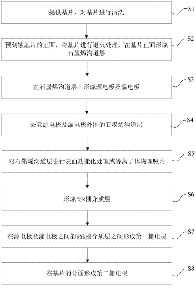
[0052] Embodiments of the present invention are described below through specific examples, and those skilled in the art can easily understand other advantages and effects of the present invention from the content disclosed in this specification. The present invention can also be implemented or applied through other different specific embodiments, and various modifications or changes can be made to the details in this specification based on different viewpoints and applications without departing from the spirit of the present invention.

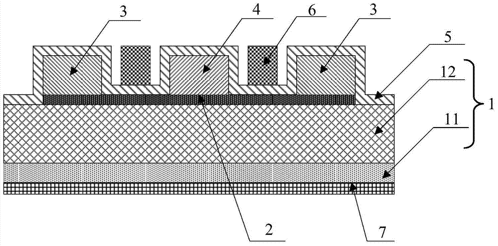
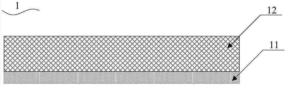
[0053] see Figure 1 to Figure 10 . It should be noted that the diagrams provided in this embodiment are only schematically illustrating the basic idea of ​​the present invention, and only the components related to the present invention are shown in the diagrams rather than the number, shape and shape of the components in actual implementation. Dimensional drawing, the type, quantity and proportion of each component can be changed arbitrarily...


PUM

PropertyMeasurementUnit
carrier mobilityaaaaaaaaaa
thicknessaaaaaaaaaa
thicknessaaaaaaaaaa

Abstract

The invention provides a double-gate and double-pole graphene field effect transistor and a manufacturing method thereof. The manufacturing method comprises the steps that a semiconductor substrate is provided, and a graphene channel layer is formed on the front face of the semiconductor substrate; a source electrode and a drain electrode are formed on the graphene channel layer; the portion, on the peripheries of the source electrode and the drain electrode, of the graphene channel layer is eliminated; surface functionalization processing or plasma physical adsorption is conducted on the graphene channel layer, and a high-k gate dielectric layer is formed; a first gate electrode is formed on the high-k gate dielectric layer between the source electrode and the drain electrode; a second gate electrode is formed on the back face of the semiconductor substrate. Graphene is directly attached to the substrate which needs graphene, troublesome transfer is not needed, and damage and impurity pollution to a graphene structure are avoided; the double-gate and double-pole graphene field effect transistor obtained through the method has the more excellent interruption performance, higher carrier mobility and smaller gate leakage current; the process procedure is simple, cost is low, and the method is suitable for large-scale production of the double-gate and double-pole graphene field effect transistor.

Description

technical field [0001] The invention belongs to the field of semiconductor devices and manufacturing, in particular to a double-gate bipolar graphene field-effect transistor and a manufacturing method thereof. Background technique [0002] Since the successful development of MOSFET devices in 1960, due to their advantages of low power consumption, high reliability, and easy size reduction, they have become an indispensable core part of advanced integrated circuits such as microprocessors and semiconductor memories, and have developed rapidly. In order to increase device density, response speed, and chip functions, scaling down of device size is a long-standing development trend of CMOS technology. That is, according to Moore's Law, the integration level of chips doubles every 18 months to 2 years. With the continuous reduction of device size in the field of microelectronics, silicon material is gradually approaching its processing limit. In order to prolong the life of Moo...

Claims


Application Information

Patent Timeline
Patent Type & Authority Applications(China)
IPC IPC(8): H01L29/78H01L21/04
CPCH01L29/66045H01L29/7831
Inventor 陈静杨燕罗杰馨柴展
Owner SHANGHAI INST OF MICROSYSTEM & INFORMATION TECH CHINESE ACAD OF SCI
Why Eureka
Try Eureka